Display Device

Active Publication Date: 2009-11-26
PANASONIC LIQUID CRYSTAL DISPLAY CO LTD +1
View PDF3 Cites 1 Cited by
  • Summary
  • Abstract
  • Description
  • Claims
  • Application Information

AI Technical Summary

Benefits of technology

[0010]The present invention was conceived in view of the above-described circumstances, and an advantage of the present invention is that a display device is provided having an array substrate in which the possibility of occurrence of the disconnection in the interlayer switching section is reduced.
[0011]In order to achieve at least the advantage described above, according to one aspect of the present invention, there is provided a display device comprising a first conductive layer in which a first electrode film is formed, a first insulating layer provided over the first conductive layer, a second conductive layer provided over the first insulating layer and in which a second electrode film is formed at a position, in plane, different from the first electrode film, and a second insulating layer provided over the second conductive layer, wherein a recess is formed over a surface of the second insulating layer, the recess having, in its inside, a first region in which the first electrode film is exposed, a second region in which the second electrode film is exposed, and a third region which connects the first region and the second region, and a conductive film is formed at least in the first through the third regions.
[0012]According to another aspect of the present invention, it is preferable that, in the display device, in the recess, a first hole which is formed through the second insulating layer and the first insulating layer and reaches the first electrode film, a second hole which is provided distanced from the first hole and which is formed through the second insulating layer and reaches the second electrode film, and a channel which connects the first hole and the second hole are formed.
[0013]According to another aspect of the present invention, it is preferable that, in the display device, the first electrode film and the second electrode film are provided with edges overlapping each other in the plane, a sloped surface extending from an inner wall of the second electrode film to an upper surface of the first electrode film is formed in the recess, and the conductive film is formed at least over the sloped surface.
[0014]According to another aspect of the present invention, it is preferable that, in the display device, in the recess, the sloped surface extends to an upper surface of the second electrode film.
[0015]According to another aspect of the present invention, it is preferable that, in the display device, the conductive film is formed at a periphery portion which is outside of an edge of the recess.

Problems solved by technology

Because of this, when a physical contact occurs in this region, there is a possibility of disconnection.

Method used


Image

  • Display Device
  • Display Device
  • Display Device

Examples


first preferred embodiment

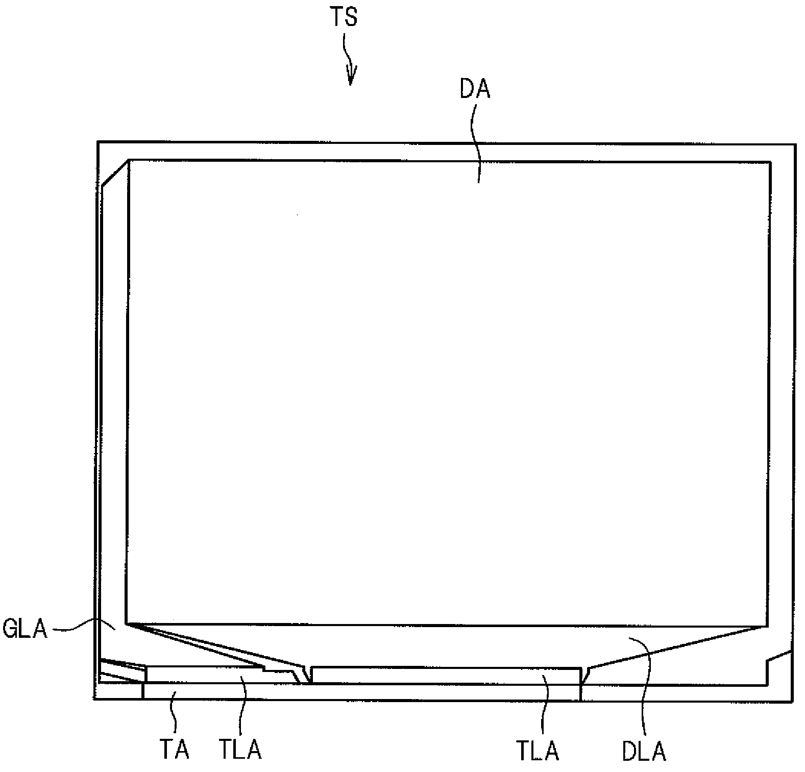
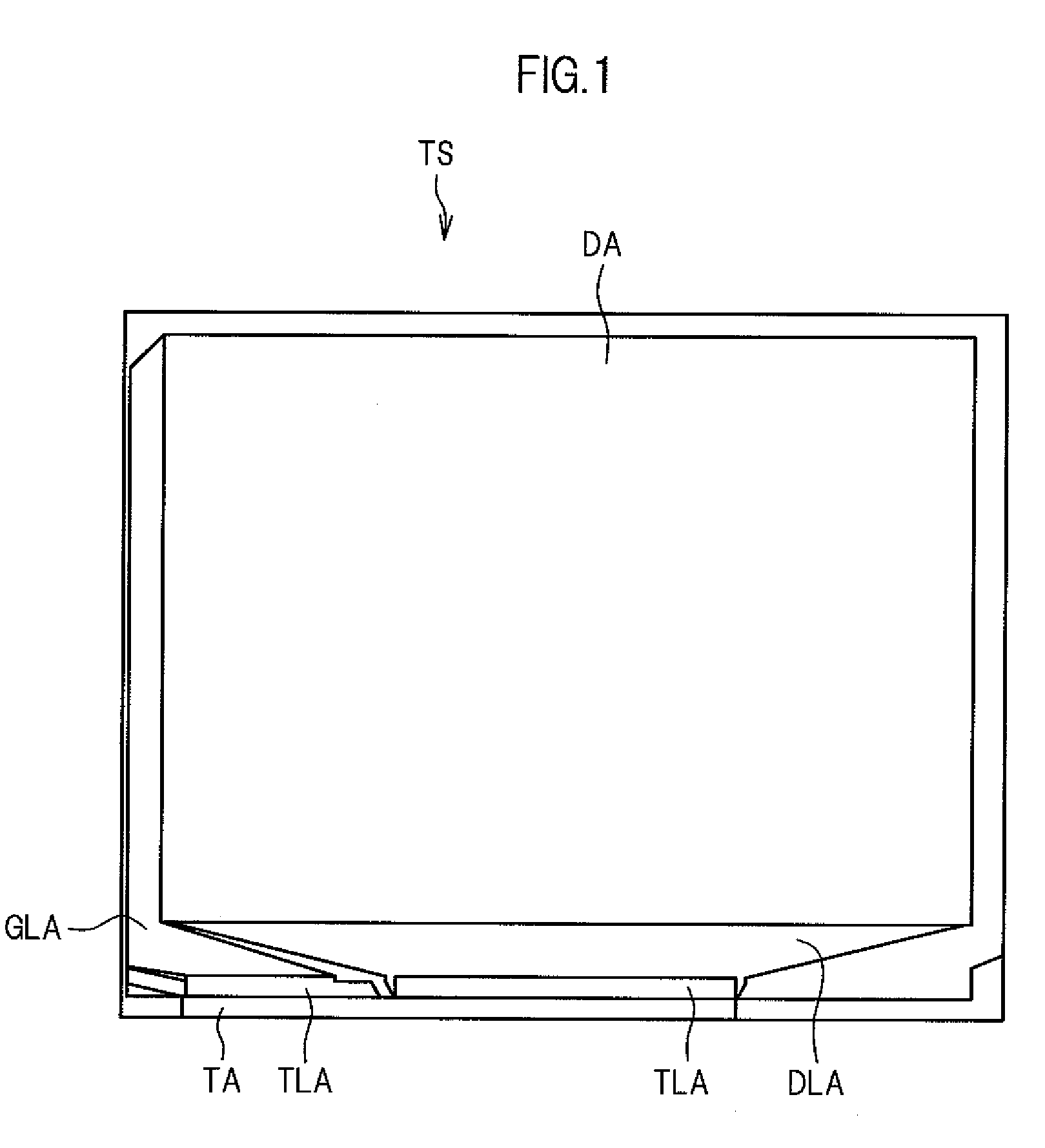
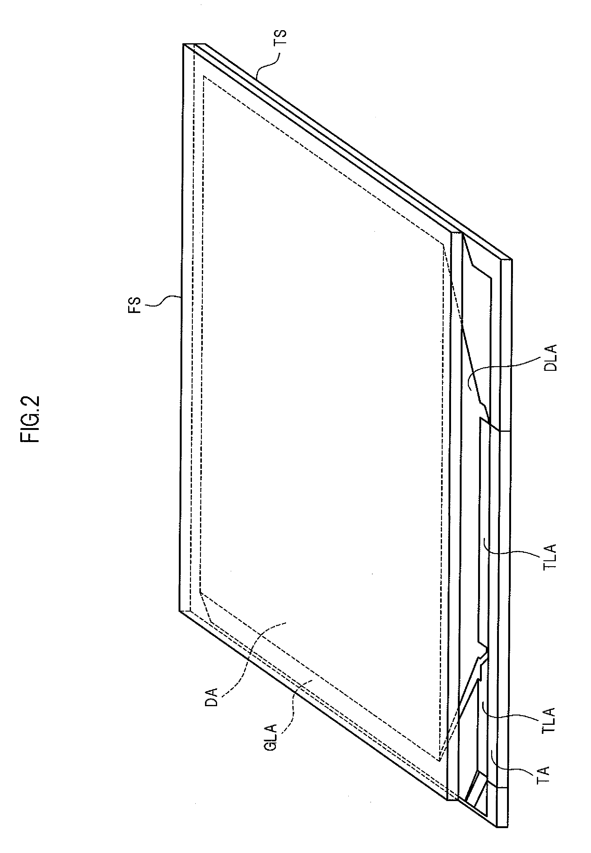
[0052]A display device according to a first preferred embodiment of the present invention is a liquid crystal display device comprising an array substrate TS, a filter substrate FS which opposes the array substrate TS and in which a color filter is provided, a liquid crystal material filled in a region sandwiched between the array substrate TS and the filter substrate FS, and a driver IC mounted on the array substrate TS. The array substrate TS and the filter substrate FS are glass substrates or the like.

[0053]FIG. 1 is a plan view showing a layout of an array substrate TS according to the preferred embodiment. Over the array substrate TS, a pixel region DA, a gate line extension region GLA, a drain line extension region DLA, a terminal portion TA, and a line region around the terminal portion TLA are placed. In the pixel region DA, aplurality of pixel circuits for displaying an image are placed. The gate line extension region GLA is provided adjacent to the pixel region DA at the l...

second preferred embodiment

[0069]As a display device according to the second preferred embodiment of the present invention has a structure similar to that in the first preferred embodiment (refer to FIGS. 1-5) except for the interlayer switching sections C1 and C2, in the second preferred embodiment, a difference from the first preferred embodiment in the structure of the interlayer switching section C1 and the manufacturing process of the array substrate TS will be primarily described.

[0070]FIG. 13 is a plan view of the interlayer switching section C1 of the second preferred embodiment. The structures to which the drain electrode film SDM and the gate electrode film GM are connected are similar to those in the first preferred embodiment. As is clear from FIG. 13, the gate electrode film GM has a region having a rectangular shape with two beveled corners in the plane. The drain electrode film SDM similarly has a region having a rectangular shape with two beveled corners in the plane. Lengths of the sides whic...

third preferred embodiment

[0074]As a display device according to a third preferred embodiment of the present invention has a structure similar to the structure of the first preferred embodiment (refer to FIGS. 1-5) except for the interlayer switching sections C1 and C2, in the following, a difference, from the first preferred embodiment, in the structure of the interlayer switching section C1 and the manufacturing process of the array substrate TS in the third preferred embodiment will be primarily described.

[0075]FIG. 16 is a plan view of the interlayer switching section C1 in the third preferred embodiment. The structures to which the drain electrode film SDM and the gate electrode film GM are connected are similar to those in the first preferred embodiment. As is clear from FIG. 16, the gate electrode film GM has a region having a rectangular shape with two beveled corners in the plane and the drain electrode film SDM has a region having a rectangular shape with two beveled corners in the plane and with t...


PUM


Abstract

A display device is provided which comprises a first conductive layer in which a first electrode film is formed, a first insulating layer provided over the first conductive layer, a second conductive layer provided over the first insulating layer and in which a second electrode film is formed at a position different, in plane, from the first electrode film, and a second insulating layer provided over the second conductive layer. Over a surface of the second insulating layer, a recess having, in its inside, a first region in which the first electrode film is exposed, a second region in which the second electrode film is exposed, and a third region which connects the first region and the second region is formed, and a conductive film is formed at least in the first through the third regions.

Description

CROSS-REFERENCE TO RELATED APPLICATION[0001]The present application claims priority from Japanese application JP 2008-137296 filed on May 26, 2008, the content of which is hereby incorporated by reference into this application.BACKGROUND OF THE INVENTION[0002]1. Field of the Invention[0003]The present invention relates to a display device, and, in particular, to a display device having a structure for electrically connecting electrode films which are formed in different layers of a substrate.[0004]2. Description of the Related Art[0005]In a display device such as a liquid crystal display device, a plurality of conductive layers are formed, with a layer of insulating material therebetween, over an array substrate forming a part of the display device. In order to electrically connect the lines existing in such a plurality of conductive layers, an interlayer switching section as shown in FIGS. 25 and 26 may be used in some cases. FIG. 25 is a plan view showing an interlayer switching s...

Claims


Application Information

Patent Timeline
IPC IPC(8): G02F1/1333B32B3/00B32B3/10
CPCG02F1/13439Y10T428/2462Y10T428/24331G02F1/1345
Inventor ISHII, MIYOYAMASHITA, MANABU
Owner PANASONIC LIQUID CRYSTAL DISPLAY CO LTD
Why Eureka
Try Eureka