Double-Sided Monolithically Integrated Optoelectronic Module with Temperature Compensation

a monolithic integrated, optoelectronic module technology, applied in the direction of lasers, electrical equipment, basic electric elements, etc., can solve the problems of difficult integration of monolithically the diode laser and the driver circuitry, the formation of fet-based driver circuitry on top of the diode laser layer is impossible, and the integration of iii-v optoelectronic components with cmos-based silicon electronics is complicated and other problems, to achiev

Active Publication Date: 2009-11-19
INNOLUME
View PDF25 Cites 3 Cited by
  • Summary
  • Abstract
  • Description
  • Claims
  • Application Information

AI Technical Summary

Benefits of technology

[0016]The optoelectronic module of the present invention preferably uses a double-sided epi-ready substrate. The optoelectronic module is preferably fabricated by epitaxially depositing the first layered structure and a protective film on the first side of the substrate, depositing the second layered structure and subsequently removing the protective film. Preferably the conditions of the deposition of the first layered structure and the protective film are selected such that the second side of the substrate remains stable and is therefore suitable for subsequent deposition of semiconductor thin films. The protective film is selected such that it is capable of protecting the first layered structure against degradation, such as decomposition, erosion and other destructive processes which can be caused by high-temperature treatment during subsequent epitaxial growth on the second side of the substrate.
[0017]The FET-based driver circuitry and the diode laser are preferably designed for high-speed operation. Close proximity between the device's parts (i.e. the diode laser, the temperature-sensitive element, and the drive circuitry as a whole) enables high-density packaging, ensures precise temperature monitoring, and may improve high-speed characteristics due to low series resistance, low cross-talks, and high-speed electronic components. An advantage is that the approach may be fully compatible with mass-production technology. The process may readily be scaled up or down as the wafer size increases or decreases with minor modification. An additional advantage of the method of the present invention is a reduction of chip area compared to a method of location of the diode laser and the driver circuitry at the same side of the substrate.

Problems solved by technology

However, it is difficult to integrate monolithically the diode laser and the driver circuitry.
For example, an integration of III-V optoelectronic components with CMOS-based (or similar) silicon electronics is a complicated problem because of the difference in lattice parameters and thermal expansion coefficients.
Therefore, formation of FET-based driver circuitry on top of the diode laser layers is impossible because FETs operating at high-frequencies are short-circuited by parallel conductivity of these conductive layers.
The most challenging part of this approach is filling the recess.
Both of these techniques are often difficult to realize taking into account a large depth of diode laser structures, especially vertical cavity surface emitting lasers.
Thus, methods for the monolithic integration of the FET-based high-speed driver circuitry and the diode laser are not well developed in the prior art.
However, in spite of certain progress in this direction, the temperature sensitivity of the laser parameters in the current state of the art is typically unsatisfactory.
Also, it is quite difficult to achieve a stabilization of the laser temperature during a long period of laser operation.
First, the ambient temperature may change rapidly and unpredictably in a wide range.
Second, the temperature of the active region of the laser affects the laser parameters.
However, use of backface monitoring does not completely solve the problem of laser output changes as a function of temperature.
In particular, this technique is incapable of adjusting the optical modulation amplitude.

Method used


Image

  • Double-Sided Monolithically Integrated Optoelectronic Module with Temperature Compensation
  • Double-Sided Monolithically Integrated Optoelectronic Module with Temperature Compensation
  • Double-Sided Monolithically Integrated Optoelectronic Module with Temperature Compensation

Examples


Embodiment Construction

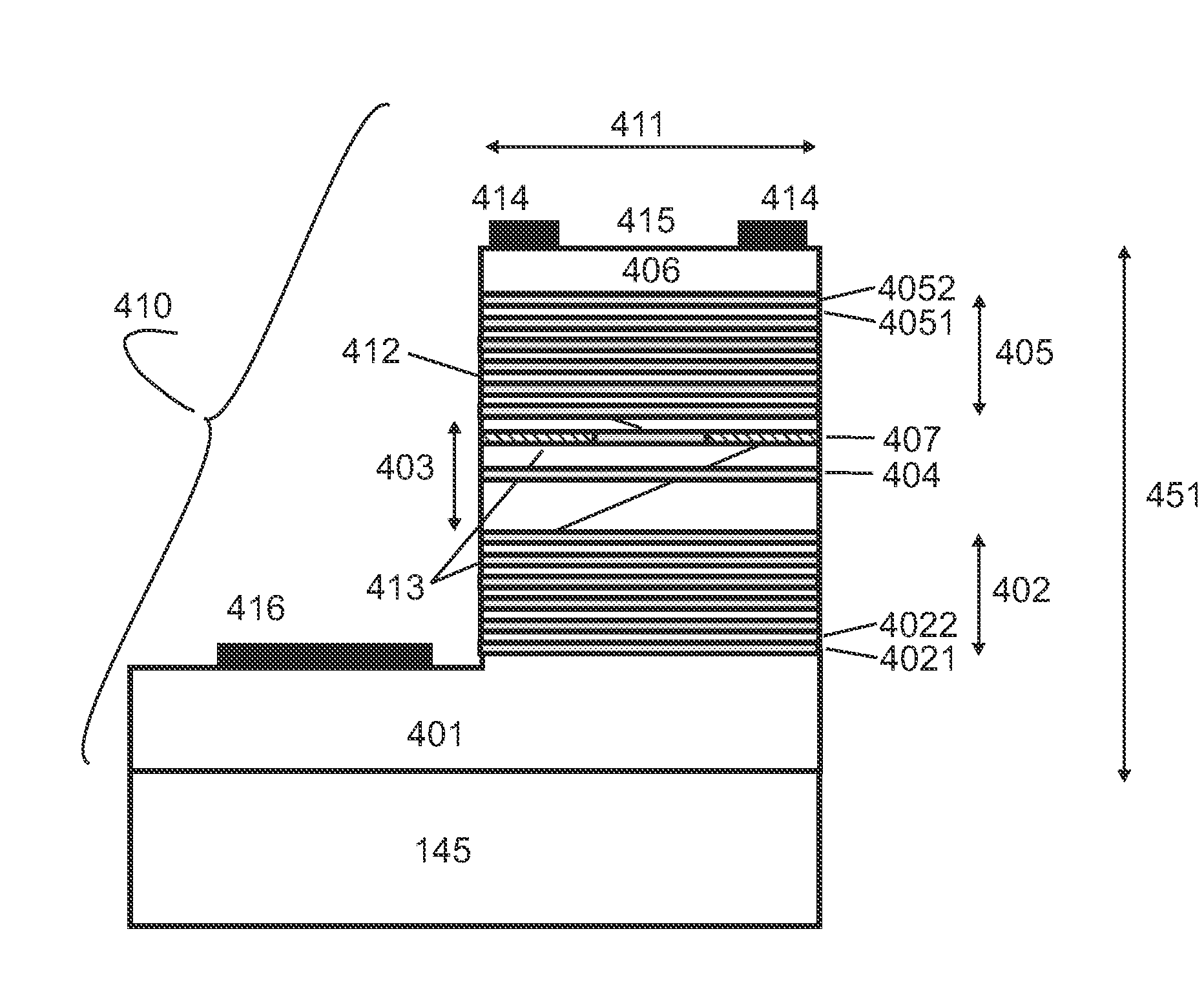
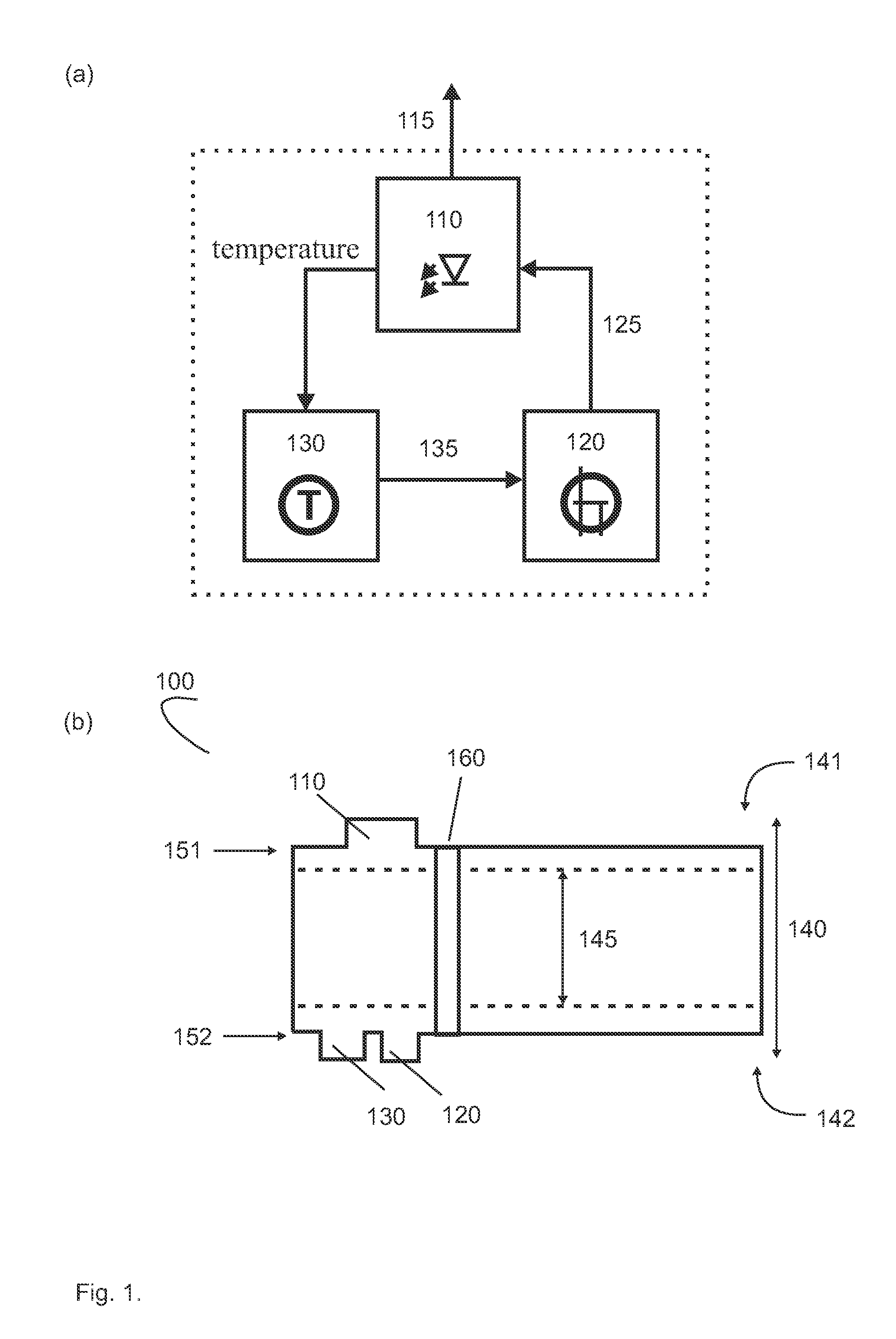
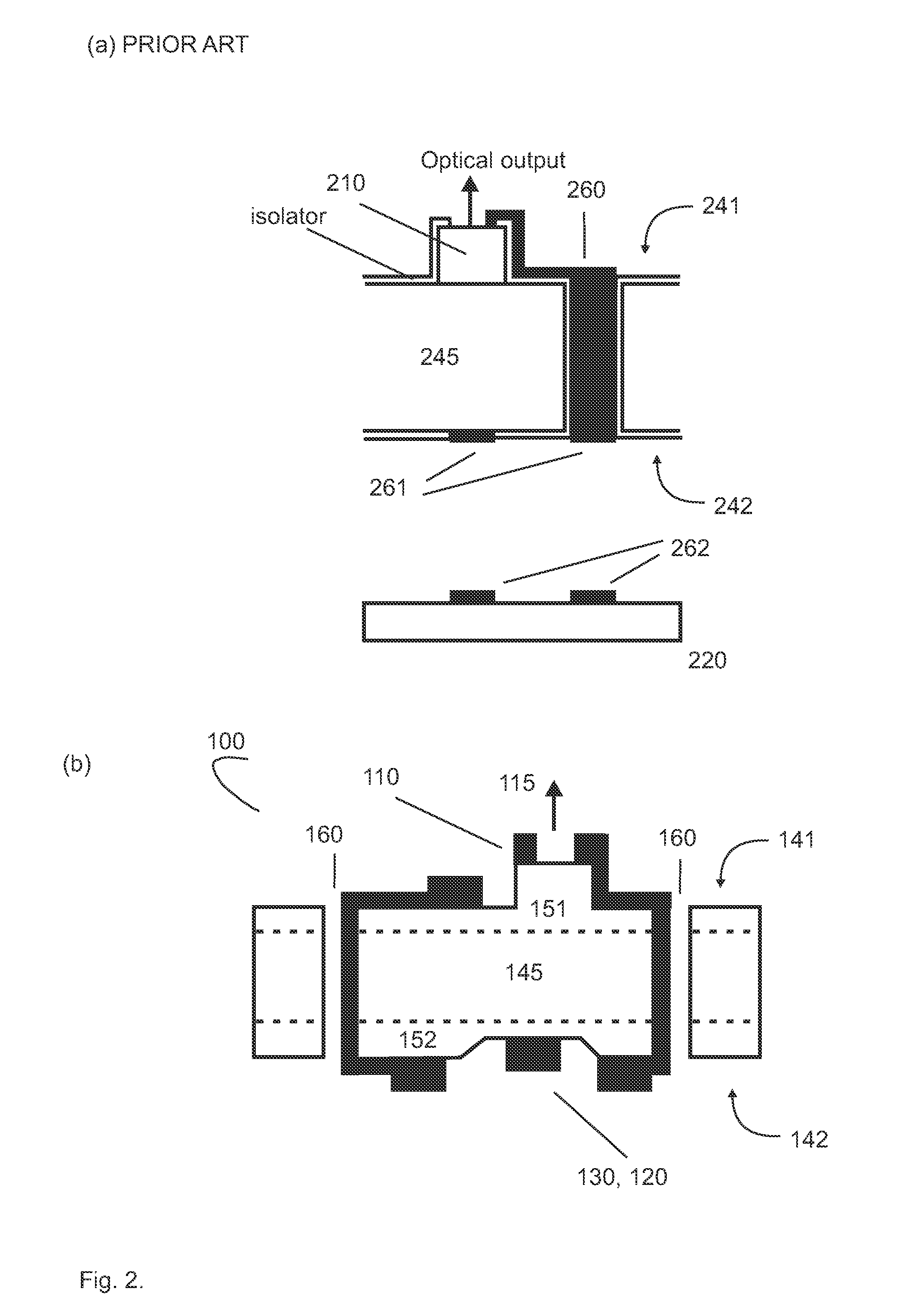
[0063]A double-sided monolithically integrated optoelectronic module (100) according to a preferred embodiment of the present invention is illustrated in FIG. 1. FIG. 1(a) illustrates the operation and a temperature compensation method of the module and FIG. 1(b) illustrates a monolithically integrated structure of the module according to one embodiment of the present invention.

[0064]The optoelectronic module (100) includes at least two parts: a driver circuitry (120) and a diode laser (110). The driver circuitry (120) produces a drive electrical signal (125) supplied to the diode laser (110), and the diode laser (110) produces an optical output (115) in response to the drive electrical signal (125).

[0065]In a preferred embodiment, the module also further includes a temperature-sensitive element (130). The temperature-sensitive element (130) is preferably fabricated in thermal contact with the diode laser (110). This means that the temperature-sensitive element is capable of produci...


PUM


Abstract

An optoelectronic module includes a semiconductor structure with a substrate having a first side and a second side, a first layered structure deposited on the first side, and a second layered structure deposited on the second side. The optoelectronic module also includes driver circuitry fabricated of the first layered structure and a diode laser fabricated of the second layered structure. The driver circuitry produces a drive electrical signal supplied to the diode laser, and the diode laser produces an optical output in response to the drive electrical signal. In a preferred embodiment, the optoelectronic module also includes a temperature-sensitive element fabricated of the first or the second layered structure. The temperature-sensitive element produces a temperature dependent control signal related to the diode laser temperature.

Description

BACKGROUND OF THE INVENTION[0001]1. Field of the Invention[0002]This invention relates to methods and devices for stabilizing a diode laser optical output with respect to temperature variations. This invention further relates to methods and devices for monolithic integration of a diode laser with a driver circuitry.[0003]2. Description of Related Art[0004]A semiconductor diode laser emits an optical output power in response to an electrical input signal. The input signal, e.g. an injection current, is applied to the laser contacts being provided by an external control circuitry, also known as laser driver circuitry. It is well recognized that co-location of electronic circuits and light-emitting devices, e.g. a driver circuitry and a diode laser, is frequently the most cost-effective solution due to the higher level of integration. However, it is difficult to integrate monolithically the diode laser and the driver circuitry. For example, an integration of III-V optoelectronic compon...

Claims


Application Information

Patent Timeline
Patent Type & Authority Applications(United States)
IPC IPC(8): H01L21/20
CPCH01S5/02248H01S5/02272H01S5/02276H01S5/02284H01S5/0261H01S5/0425H01S5/06804H01L2924/12032H01L2224/48091H01S5/18311H01L2924/00014H01L2924/00H01L24/73H01L2224/73257H01L2924/13063H01L2924/14H01S5/04254H01S5/04257H01S5/02251H01S5/02325H01S5/02345H01S5/0237
Inventor KRESTNIKOV, IGORKURB, JURGENKOVSH, ALEXEYZHUKOV, ALEXEYLIVSHITS, DANIILMIKHRIN, SERGEY
Owner INNOLUME
Why Eureka
Try Eureka