Flexible piezoresistive interfacial shear and normal force sensor and sensor array
a technology of piezoresistive interfacial shear and normal force, which is applied in the direction of force/torque/work measurement apparatus, instruments, applications, etc., can solve the problems of pressure ulcers associated with diabetic foot, inability to measure the shear force component simultaneously,
- Summary
- Abstract
- Description
- Claims
- Application Information
AI Technical Summary
Problems solved by technology
Method used
Image
Examples
example 1
An Array of Force Sensors
[0068]A 16×16 2D array of force sensors was built for pressure mapping applications. A zero-potential scanning method was used to address individual elements that were on the intersections of row and column electrodes, as depicted in FIG. 7.
[0069]A zero-potential scanning method was based on turning off the unspecified row and column electrodes to have current only flow through the specified row to column electrical path, which eliminated cross-talk paths. The row electrodes were turned off with multiplexed switches, and the column electrodes were turned off with virtual ground from the amplifier. Each row-column cross had a piezoresistor connected for scanning. The scanned analog data was amplified, sent to an analog-to-digital (A / D) converter, saved in a microcontroller unit (MCU), and sent to a computer by recommended standard 232 (RS-232) or universal serial bus (USB). Software processed the data to show the pressure-mapping image of shear and normal for...
example 2
Shadow Masking Technique
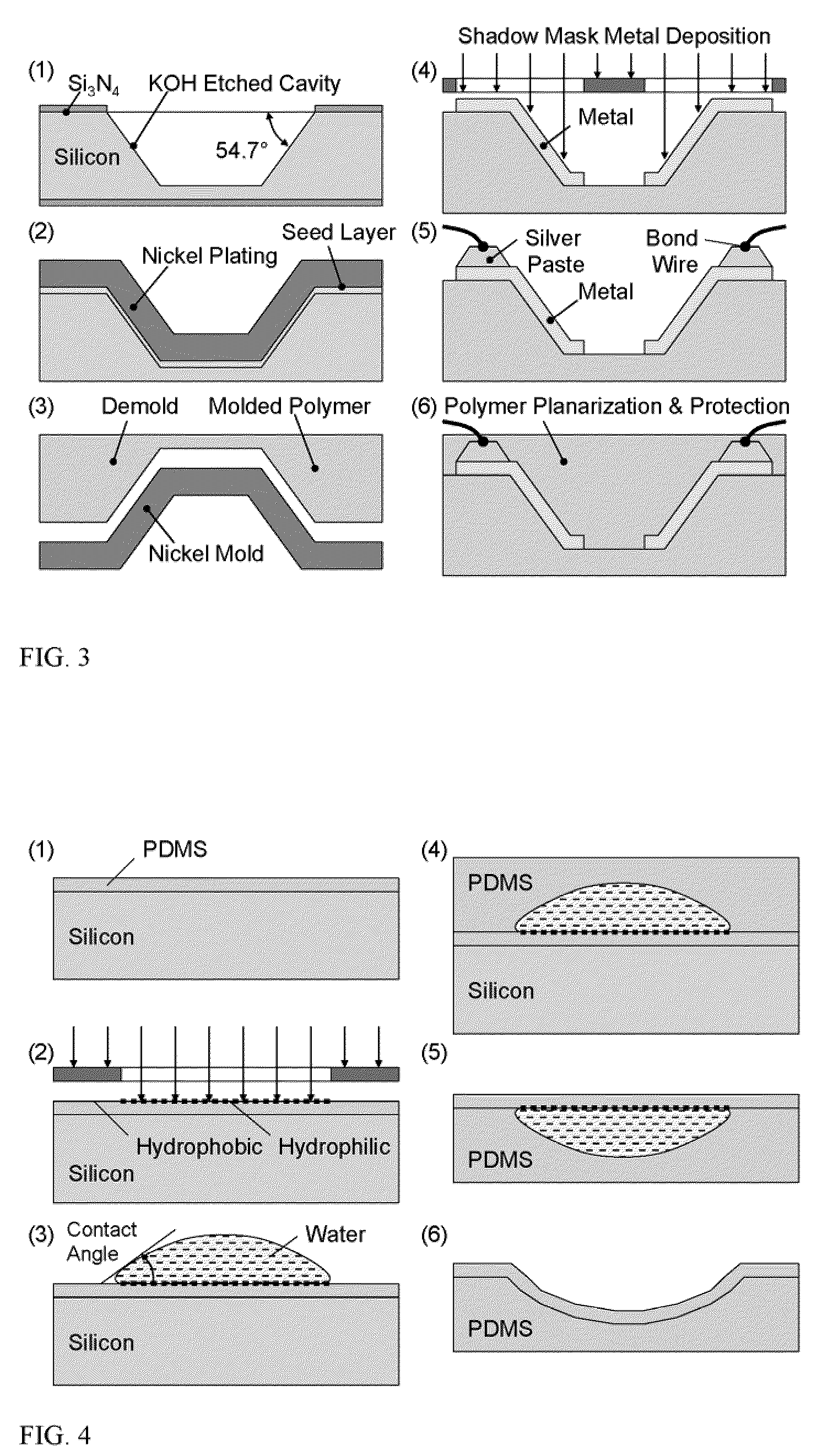
[0071]A shadow mask was made by wet etching of a stainless steel film with a thickness of 50 μm and a line width of 100 μm. A thin layer of PDMS film was made by coating the Dow Corning Sylgard 184 PDMS pre-polymer and its curing agent mixture on a glass substrate, and then curing at an elevated temperature of 70° C. in a convection oven. The cured PDMS film was subsequently covered with the shadow mask for sputtering with a thin layer of gold around 20 nm. A pair of piezoresistors was patterned on a piece of PDMS film, as depicted in FIG. 9A, where a 20-cent Hong Kong coin was used as a size reference. Various designs of piezoresistor pairs were deposited on the PDMS film, as depicted in FIG. 9B, which shows a 2-D force sensor array.
PUM
| Property | Measurement | Unit |
|---|---|---|
| angle | aaaaa | aaaaa |
| angle | aaaaa | aaaaa |
| tilt plane angle | aaaaa | aaaaa |
Abstract
Description
Claims
Application Information
 - R&D
- Intellectual Property
- Life Sciences
- Materials
- Tech Scout
- Unparalleled Data Quality
- Higher Quality Content
- 60% Fewer Hallucinations
Browse by: Latest US Patents, China's latest patents, Technical Efficacy Thesaurus, Application Domain, Technology Topic, Popular Technical Reports.
© 2025 PatSnap. All rights reserved.Legal|Privacy policy|Modern Slavery Act Transparency Statement|Sitemap|About US| Contact US: help@patsnap.com


