
Apparatus, system, and method for bad block remapping

a technology of block remapping and applicability, applied in the field of solid-state storage, can solve the problems of introducing data errors, affecting the reliability of data storage, and failure of specific regions of solid-state storage, and achieve the effect of high reliability and high reliability

Active Publication Date: 2009-11-12
SANDISK TECH LLC
View PDF29 Cites 166 Cited by
  • Summary
  • Abstract
  • Description
  • Claims
  • Application Information

AI Technical Summary

Benefits of technology

[0008]From the foregoing discussion, it should be apparent that a need exists for an apparatus, system, and method that provide a highly reliable way to manage bad blocks in solid-state st

Problems solved by technology

Solid-state storage, as well as other forms of data storage media, is subject to failures of specific regions within the solid-state storage.
This type of failure may result in loss of ability to store data in the specific failed region, but rest of the solid-state storage may function normally.
Allowing the failed region to be used for data storage would introduce data errors.
If a particular physical erase block in a solid-state storage array fails, a logical erase block that includes the failed physical erase block may be unavailable unless another physical erase block is substituted for the failed physical erase block.
Bad blocks in solid-state storage, such as NAND flash memory, are common and solid-state storage elements often come from the factory with bad erase blocks.
Solid-state storage may be used as log storage system and not as a random access device so bad block mapping schemes developed for disks and other data storage devices may be inadequate.
Solid-state storage typically also has a wear-out mechanism so areas used frequently may be subject to failure before other areas in the solid-state storage.
Traditional bad block management techniques are inadequate for providing highly reliable bad block management for solid-state storage.

Method used


Image

  • Apparatus, system, and method for bad block remapping
  • Apparatus, system, and method for bad block remapping
  • Apparatus, system, and method for bad block remapping

Examples


Embodiment Construction

[0041]Many of the functional units described in this specification have been labeled as modules, in order to more particularly emphasize their implementation independence. For example, a module may be implemented as a hardware circuit comprising custom VLSI circuits or gate arrays, off-the-shelf semiconductors such as logic chips, transistors, or other discrete components. A module may also be implemented in programmable hardware devices such as field programmable gate arrays, programmable array logic, programmable logic devices or the like.

[0042]Modules may also be implemented in software for execution by various types of processors. An identified module of executable code may, for instance, comprise one or more physical or logical blocks of computer instructions which may, for instance, be organized as an object, procedure, or function. Nevertheless, the executables of an identified module need not be physically located together, but may comprise disparate instructions stored in d...


PUM


Abstract

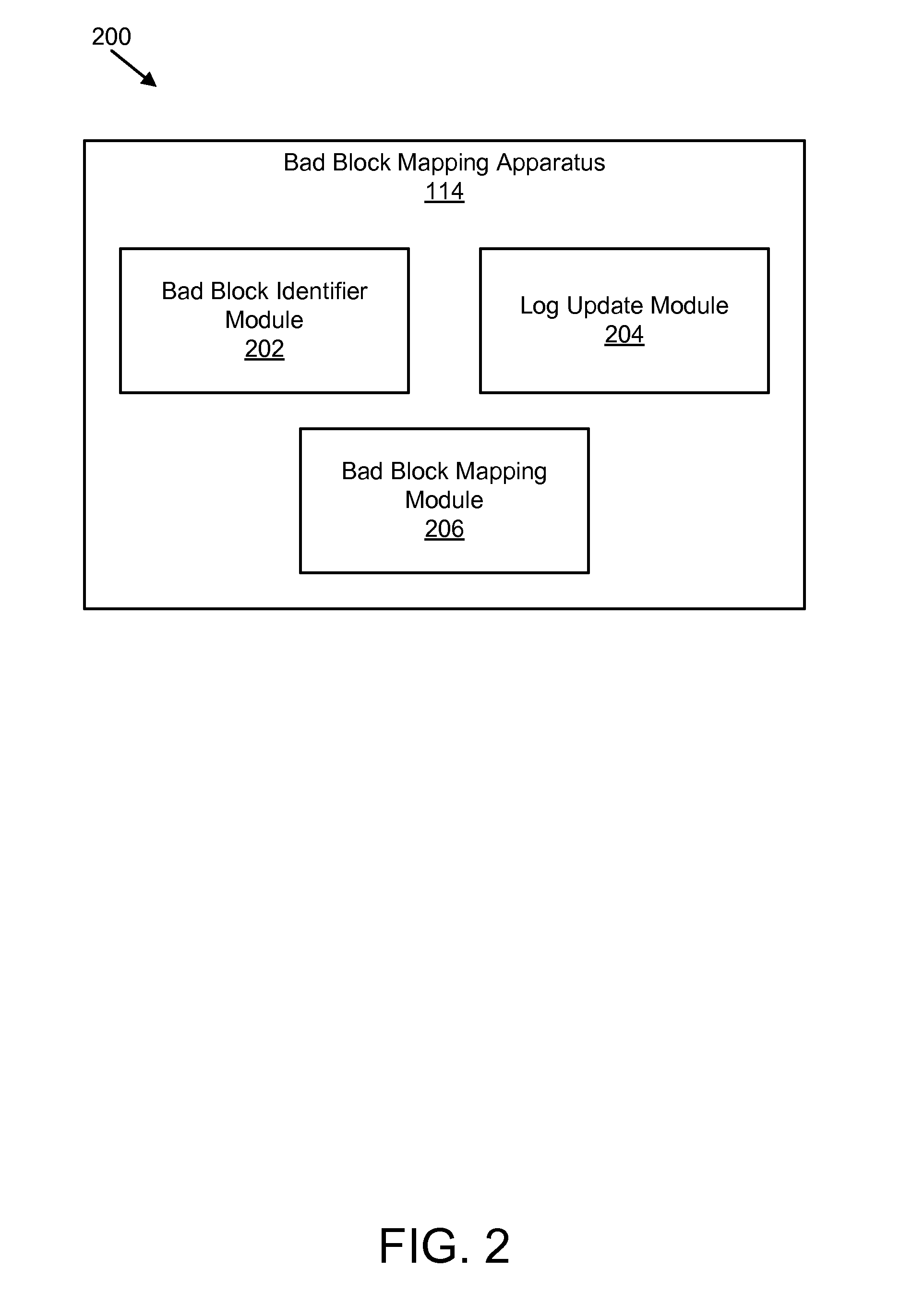
An apparatus, system, and method are disclosed for bad block remapping. A bad block identifier module identifies one or more data blocks on a solid-state storage element as bad blocks. A log update module writes at least a location of each bad block identified by the bad block identifier module into each of two or more redundant bad block logs. A bad block mapping module accesses at least one bad block log during a start-up operation to create in memory a bad block map. The bad block map includes a mapping between the bad block locations in the bad block log and a corresponding location of a replacement block for each bad block location. Data is stored in each replacement block instead of the corresponding bad block. The bad block mapping module creates the bad block map using one of a replacement block location and a bad block mapping algorithm.

Description

CROSS-REFERENCES TO RELATED APPLICATIONS[0001]This application claims priority to U.S. Provisional Patent Application No. 61 / 042,738 entitled “Apparatus, System, and Method for Bad Block Remapping” and filed on Apr. 5, 2008 for David Flynn, et al., which is incorporated herein by reference.FIELD OF THE INVENTION[0002]This invention relates to solid-state storage and more particularly relates to bad block remapping in solid-state storage.BACKGROUNDDescription of the Related Art[0003]Solid-state storage, as well as other forms of data storage media, is subject to failures of specific regions within the solid-state storage. This type of failure may result in loss of ability to store data in the specific failed region, but rest of the solid-state storage may function normally. Allowing the failed region to be used for data storage would introduce data errors.[0004]Memory cells in solid-state storage are typically arranged in some type of a matrix of rows and columns. Regions may further...

Claims


Application Information

Patent Timeline
IPC IPC(8): H03M13/05G06F11/22G06F11/07
CPCG06F11/006G06F11/1068G11C29/76G06F11/1666G06F11/1435G06F12/0246G06F2212/1016G06F2212/1032G06F2212/7205G06F2212/7207
Inventor FLYNN, DAVIDTRASSER, JOHNTHATCHER, JONATHANATKISSON, DAVIDZAPPE, MICHAELAUNE, JOSHUAVIGOR, KEVIN
Owner SANDISK TECH LLC
Learn More