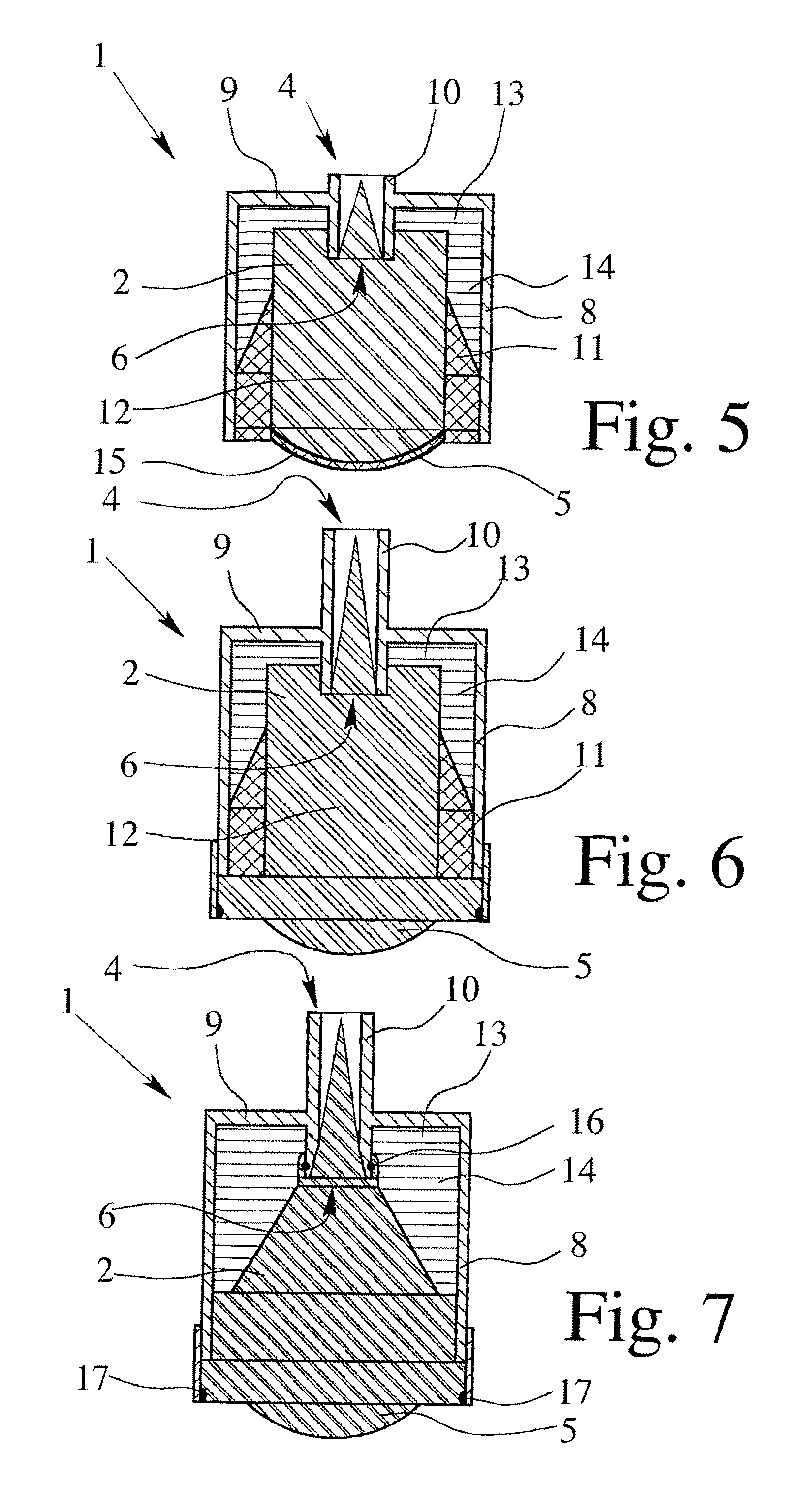
[0012]The above object is first and essentially met with the dielectric antenna in question in that the dielectric body has essentially the cross-section of the radiation opening in the area of the supply section. It is, thereby, achieved that the dielectric body is no longer subject to appreciable cross-section changes over its entire extent in the main radiation direction, so that it ultimately fills up the radiation opening in the radiation section. In particular, it is not necessary, for example, to produce a tapered dielectric body and a tapered conductive sheath corresponding to this tapered dielectric body. The dielectric antenna formed according to the invention can be produced with considerably less effort than known constructions. Though slightly more dielectric material is needed to produce the dielectric body, the advantages balance this out, by far.
[0015]Preferably, the supply section is additionally formed by a
waveguide, which is attached to the conductive sheath on the outside and at the supply opening or which is inserted in the supply opening in the conductive sheath and then preferably extends into the dielectric body. In both cases, a connection to an electromagnetic supply source can be made in a simple manner.
[0016]The lens-shaped radiation section in the dielectric antenna according to the invention is fundamentally disengaged so that electromagnetic
waves are emitted from the radiation section having an even as possible
phase front. Here, it is to be taken into consideration that in order to achieve an even
phase front, the runtimes of the different parts of the electromagnetic radiation from the supply section to the different spots of the lens surface of the radiation section have to be approximately the same and that the
refraction of the electromagnetic radiation resulting at the transition from the surface of the dielectric body in the radiation section to the
outer space has to take place due to the dielectricity transfer between the dielectric body and the
outer space in the direction of the main radiation direction, so that good directional characteristics result.
[0019]Using this measure, the electromagnetic radiation reaches the radiation area directly—without previous reflection—which previously, without the low-
permittivity boundary area, struck the sidewall of the conductive sheath. Furthermore, the electromagnetic radiation hitting the boundary area of the radiation section of the dielectric body arrives at a shallower angle than is the case in dielectric bodies that consist of a uniform dielectric. For this reason, only a comparably lower correction of the radiation path is necessary by the lens-shaped radiation section, so that the
lens thickness can be considerably less in total. Furthermore, the antenna can be built distinctly shorter in the main radiation direction in order to illuminate the same radiation opening and to achieve the same directional characteristics as comparably longer conventional dielectric antennae. The results of this measure are short-built dielectric antennae having very
flat lens geometry.
[0021]In order to avoid losses when the electromagnetic radiation from the supply section enters into the dielectric body, the absorber layer is, in particular, adjacent to the conductive sheath and, in particular, not provided in the primary
strong field area of the dielectric body. The term “primary
strong field area” is used for the area that is impinged directly—i.e., without consideration of reflection—by electromagnetic radiation. Thus, it is ensured that, in the dielectric body, only reflected electromagnetic radiation—e.g., from the conductive sheath—is reflected onto the absorber layer and cannot be reflected any longer. Reflections are often not desired because they can lead to
noise in the emission
signal and to echoes in the emission signals to be evaluated and make the evaluation of the electromagnetic radiation emitted and received by the dielectric antenna more difficult.
[0022]In a further preferred embodiment of the invention, the dielectric body has a side absorber layer in a boundary section adjacent to the conductive sheath, which is provided, in particular, in the boundary section to the sidewall of the conductive sheath and, in particular, is not in the primary
strong field area of the dielectric body. This side absorber layer makes it possible to absorb reflected and to be reflected electromagnetic radiation emitted in the direction of the sidewall of the conductive sheath and, thus, to avoid further reflection. It is of particular
advantage, here, when the side absorber layer is arranged adjacent to the supply-side absorber layer in the supply section of the dielectric body. In particular, this is advantageous in view of producing such an absorber layer.