
Radio frequency (RF) integrated circuit (IC) packages with integrated aperture-coupled patch antenna(s) in ring and/or offset cavities

a technology of integrated circuits and radio frequency, applied in the field of communication circuitry, can solve the problems of high cost, high cost, and difficult consumer pointing antennas, and achieve the effect of reducing the number of components

Active Publication Date: 2009-10-15
GLOBALFOUNDRIES US INC
View PDF18 Cites 139 Cited by
  • Summary
  • Abstract
  • Description
  • Claims
  • Application Information

AI Technical Summary

Benefits of technology

[0009]One or more embodiments of the invention are suitable for automatic processes and reduce the number of components previously involved with packaging antennas.

Problems solved by technology

These systems are often assembled using expensive and bulky waveguides and package-level or board-level microstrip structures to interconnect semiconductors and their required transmitter-or receiver-antennas.
However, high gain antennas for wireless video applications have very narrow beam widths, so pointing the antenna is very difficult for consumers.
However, packaging RF chips with integrated antennas or phased arrays is extremely difficult and very expensive due to the expensive components and extensive labor involved.

Method used


Image

  • Radio frequency (RF) integrated circuit (IC) packages with integrated aperture-coupled patch antenna(s) in ring and/or offset cavities
  • Radio frequency (RF) integrated circuit (IC) packages with integrated aperture-coupled patch antenna(s) in ring and/or offset cavities
  • Radio frequency (RF) integrated circuit (IC) packages with integrated aperture-coupled patch antenna(s) in ring and/or offset cavities

Examples


Embodiment Construction

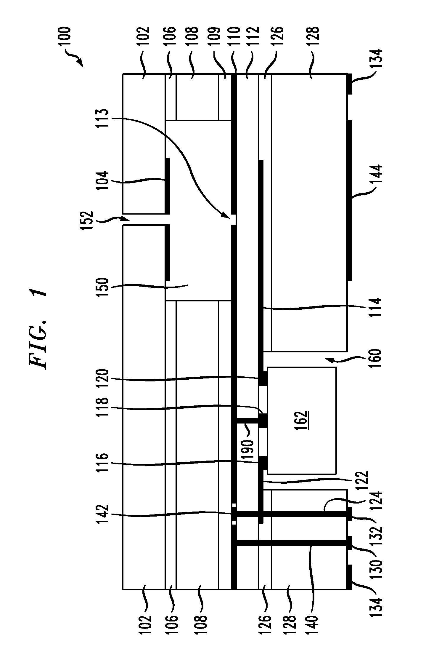
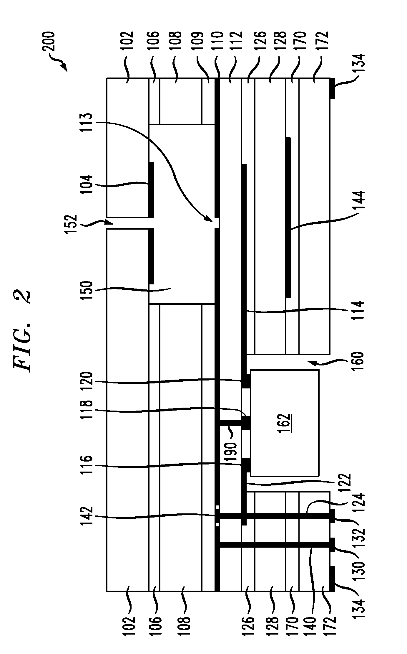
[0029]One or more embodiments of the invention provide an apparatus and method for low cost packages with integrated antennas and phased arrays operating in the millimeter wave (mmWave) range. An exemplary inventive package with integrated antennas is based on a multilayer printed circuit board (PCB). The package contains, for example, a rectangular or ring cavity for implementing high performance antenna(s) or antenna arrays and another cavity housing mmWave radio frequency (RF) integrated circuit chips. One or more embodiments of the invention also provide techniques to overcome the difficulties in making internal cavities and to avoid the need to employ wire bond technology at mmWave frequencies. Embodiments of the inventive packaging technology are consistent with the PCB manufacturing process and can be used for packages with an integrated antenna or antenna array.

[0030]Instances of the invention thus provide low cost packaging with integrated antennas or planar phased arrays; ...


PUM


Abstract

A radio-frequency integrated circuit chip package has N integrated aperture-coupled patch antennas, N being at least two, and includes N generally planar patches, and at least one generally planar ground plane spaced inwardly from the N generally planar patches and substantially parallel thereto. The ground plane is formed with at least N coupling aperture slots therein, and the slots are substantially opposed to the patches. N feed lines are spaced inwardly from the ground plane and substantially parallel thereto, and at least one radio frequency chip is spaced inwardly from the feed lines and coupled to the feed lines and the ground plane. A first substrate layer is spaced inwardly from the feed lines, and is formed with a chip-receiving cavity, with the chip located in the chip-receiving cavity. A second substrate layer is interposed in a region between the ground plane and a plane defined by the patch, the patch is formed in a first metal layer, the ground plane is formed in a second metal layer, and the second substrate layer defines an antenna cavity in which the N generally planar patches are located. “Island” and “offset” configurations, as well as fabrication methods, are also disclosed.

Description

FIELD OF THE INVENTION[0001]The present invention generally relates to communications circuitry, and, more particularly, to radio frequency (RF) integrated circuit (IC) packages.BACKGROUND OF THE INVENTION[0002]In a wireless network, the connectivity and communication between devices is achieved through antennas attached to receivers or transmitters, in order to radiate the desired signals to or from other elements of the network. In radio communication systems, such as millimeter-wave radios, discrete components are usually assembled with low integration levels. These systems are often assembled using expensive and bulky waveguides and package-level or board-level microstrip structures to interconnect semiconductors and their required transmitter-or receiver-antennas. With recent progress in semiconductor technology and packaging engineering, the dimensions of these radio communication systems have become smaller. For applications such as wireless universal serial bus (USB), the op...

Claims


Application Information

Patent Timeline
IPC IPC(8): H01Q9/04H01P11/00
CPCG06K19/07749Y10T29/49016H01L23/3121H01L23/66H01L2223/6677H01L2224/16H01L2924/01079H01L2924/09701H01Q1/38H01Q21/065H01Q1/2283H01Q9/0457H01Q21/061H01Q23/00G06K19/07786H01L2224/16227H01L2924/15153H01L2924/15323
Inventor AKKERMANS, JOHANNES A.G.FLOYD, BRIAN A.LIU, DUIXIAN
Owner GLOBALFOUNDRIES US INC
Learn More