
Semiconductor memory device having high stability and quality of readout operation

a memory device and memory technology, applied in the field of semiconductor memory devices, can solve the problems of deteriorating access time, access margin, and pn-junction potential gradient being particularly steep, and applying this method cannot completely negate the influence of interferential current, so as to achieve fast and stable operation, eliminate interference current, and eliminate interference current

Inactive Publication Date: 2009-10-01
LAPIS SEMICON CO LTD
View PDF3 Cites 6 Cited by
  • Summary
  • Abstract
  • Description
  • Claims
  • Application Information

AI Technical Summary

Benefits of technology

[0029]It is therefore an object of the present invention to provide a semiconductor memory device including memory cells, each of which outputs two or more bits of data per direction, operating fast and stably with an interferential current eliminated.
[0032]In a semiconductor memory device in accordance with the present invention, the biasing condition is appropriately applied to the memory cell array as described above, thus eliminating the interferential current conventionally problematic to thereby accomplish the fast and stable operation. This is applicable to the readout operation for two or more bits of data per direction of a memory cell.
[0033]Further, in accordance with the present invention, each of the plurality of sub-blocks may have a predetermined number of memory cells and be sectioned into a plurality of regions arranged in hierarchy. Thus, in addition to eliminating the interferential current to allow the fast and stable operation, the source and drain selectors are separately controlled from each other, simplifying the circuit configuration for supplying the first voltage and minimizing the area required for the memory cell array.

Problems solved by technology

The potential gradient at the PN-junction thereby becomes especially steep in the vicinity of the gate electrode due to the negatively biased gate electrode.
However, even applying this method cannot completely negate the influence of the interferential current.
These phenomena, from the viewpoint of power supply voltage and timing, deteriorate the access time, and hence access margin, to a remarkable extent.
As described above, the conventional semiconductor memory devices have a problem such that an interferential current flows to other multi-valued memory cells connected to a selected word line to exert a bad influence on the fast readout operation or operational margin.
As a result, between the sub-bit line used for readout and the biased main bit line, a bit line exists which may cause floating, thus enabling an interferential current to flow until this bit line is charged, which is also problematic.
Because of the problems, it is indeed difficult in the solution by Tanaka to, solve the problems.

Method used


Image

  • Semiconductor memory device having high stability and quality of readout operation
  • Semiconductor memory device having high stability and quality of readout operation
  • Semiconductor memory device having high stability and quality of readout operation

Examples


Embodiment Construction

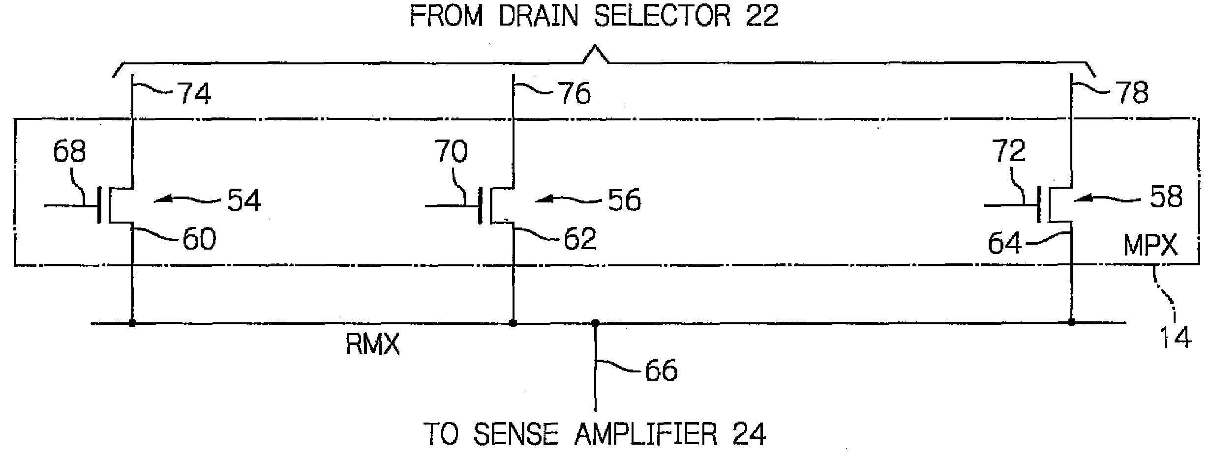
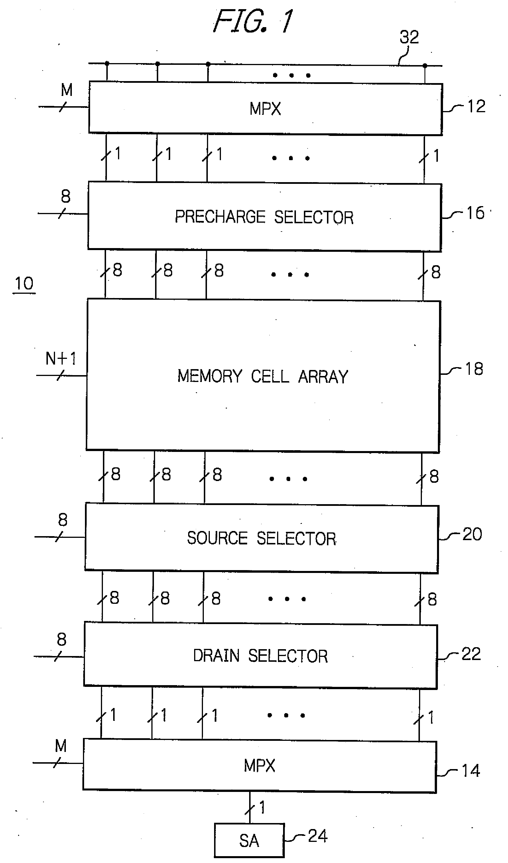
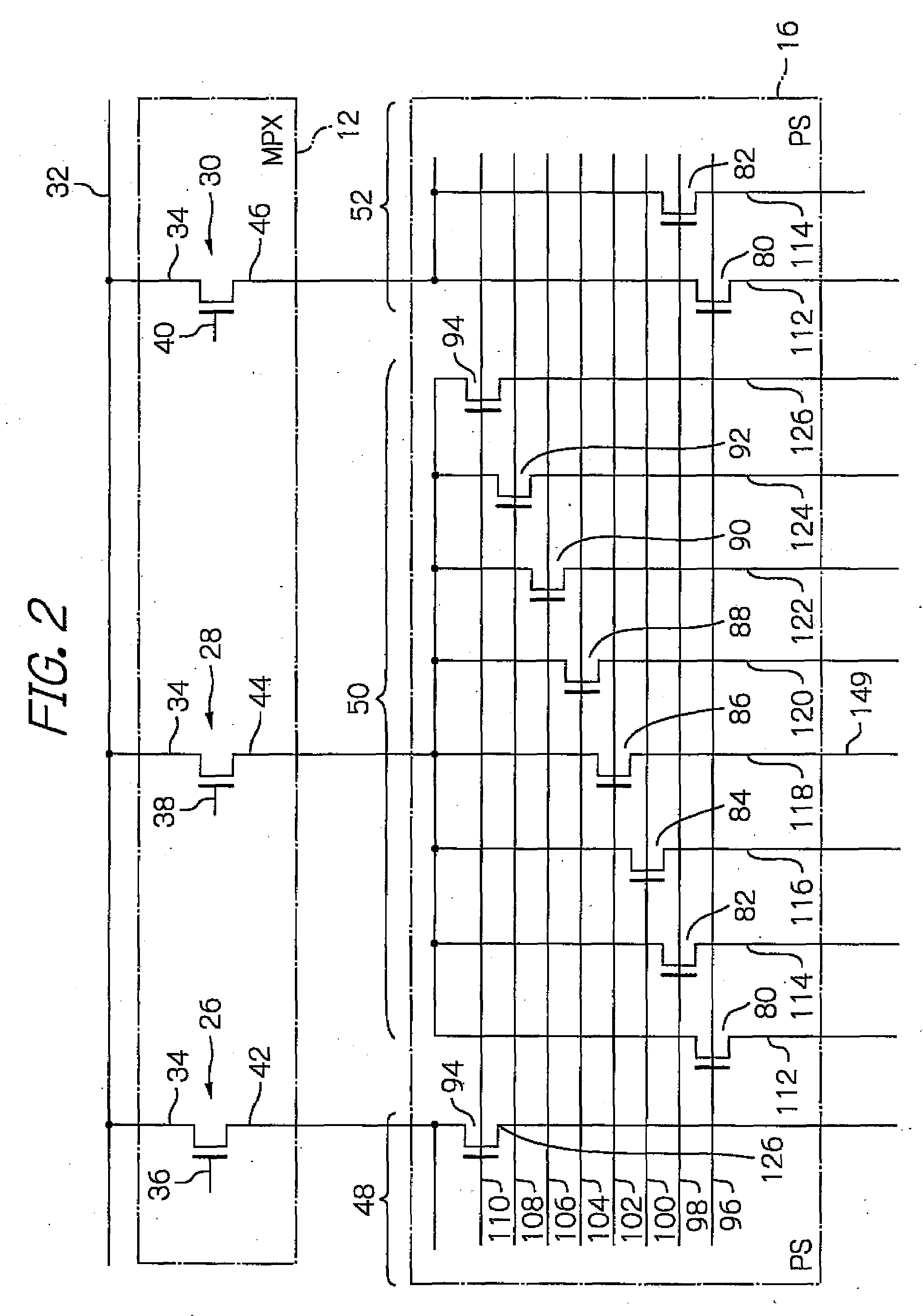
[0051]Well, reference will be made to accompanying drawings to describe a semiconductor memory device in accordance with preferred embodiments of the present invention. With reference first to FIG. 1, in a semiconductor memory device 10 in accordance with a preferred embodiment, a sense amplifier 24 is adapted to detect either a voltage level on or a current flowing over a column line; and, when reading out a stored content, or data, in a multi-valued memory cell of the memory cell device 10, a multiplexer (MPX) 14 selects a sub-block including one of the memory cells, which has data to be read out stored, in a row, a drain selector (DS) 22 selects a first column line connected to one terminal of the memory cell having the data to be read out, a precharge selector 16 selects a second column line connected to the other terminal of one of the memory cells which adjacent to the one terminal of the memory cell having the data to be read out, another multiplexer 12 selects a sub-block in...


PUM


Abstract

A semiconductor memory cell device includes a first multiplexer selecting a sub-block including a memory cell storing data to be read out in a row, a drain selector selecting a first column line connected to one terminal of the memory cell to be read, a precharge selector selecting a second column line connected to the other terminal of the memory cells adjacent to the one terminal of the memory cell storing the data to be readout, a second multiplexer selecting the sub-block including the second column line, a source selector selecting a third column line connected to the other terminal of the memory cell storing the data to be read out. The second multiplexer and precharge selector, when selecting, apply a first voltage to the second column line, and the source selector, when selecting, applies a second voltage to the third column line.

Description

BACKGROUND OF THE INVENTION[0001]1. Field of the Invention[0002]The present invention relates to a semiconductor memory device, and more particularly to a semiconductor memory device having nonvolatile memory cells to which a voltage is applied to read out data stored therein.[0003]2. Description of the Background Art[0004]Conventionally, various types of flash memory have been proposed, one of which is of a so-called “multi-valued memory cell”. The “multi-valued memory cell” may be a nonvolatile memory cell which can store two kinds of data and output the stored data in different directions. The flash memory may often include an array of multi-valued memory cells aligned in the form of matrix. Technique employed for such flash memories is disclosed by, for example, U.S. Patent Application Publication Nos. US2005 / 0265107 A1 to Tanaka and US2006 / 0239059 A1 to Murata.[0005]The memory cell array circuit taught by Murata is formed into a plurality of sub-blocks, each of which includes e...

Claims


Application Information

Patent Timeline
Patent Type & Authority Applications(United States)
IPC IPC(8): G11C7/00G11C8/00
CPCG11C8/10G11C11/5642G11C2211/5634G11C16/26G11C16/24
Inventor MATSUI, KATSUAKIOGANE, JUNICHI
Owner LAPIS SEMICON CO LTD
Learn More