
Method of making and designing lead frames for semiconductor packages

a lead frame and semiconductor technology, applied in semiconductor devices, semiconductor/solid-state device details, electrical devices, etc., can solve the problems of lack of structural rigidity, lack of rigidity, thinness, etc., and achieve the effect of avoiding bending, avoiding bending, and avoiding bending

Active Publication Date: 2009-09-24
SEMICON COMPONENTS IND LLC
View PDF7 Cites 4 Cited by
  • Summary
  • Abstract
  • Description
  • Claims
  • Application Information

AI Technical Summary

Benefits of technology

[0010]The present invention provides etching a pattern onto a lead frame from the bottom and from the top where an IC will be mounted. Cavities are formed by the bottom etching that do not penetrate through the lead frame. These cavities may then be filled with a pre-mold material. Then, illustratively, the top surface is etched to a designed pattern. However, in contrast to prior art, the top is etched completely through the lead frame to the pre-mold material. This etching may be used to remove the lead frame material that joins several lead frames to each other. This removes any metal joining the lead frames to each other and accommodates later singulation. In such an instance the pre-mold material provides the structural rigidity and stability to the lead frames.
[0012]The present invention provides for the electrical connections of the lead frame to be completed before the IC is mounted. This advantageously allows a flexibility of locating the lead frame runs not found in the prior art, where the electrical isolation of the lead frame runs is accomplished after the IC is mounted.
[0014]Reiterating the present invention provides an advantage in the flexibility of locating the etch leads on the lead frame.

Problems solved by technology

One continuing problem is the lead frame included etched leads that must be electrically isolated from all the other leads coming from an IC.
This need results in very thin, flimsy leads that lack structural rigidity and difficult to hold in place for either wire bonding or flip chip bonding.
This singulation is accomplished by cutting with a saw, and sawing leads to quality problems, e.g., delamination, etc.
One limitation of the '116 patent is that the metal interconnected web restricts where the etched leads may run with respect to the chip and where the other leads may run.
For example, since web is of the metal it may be inconvenient, difficult or impossible to design long runs beneath the IC or runs that cross each other.

Method used


Image

  • Method of making and designing lead frames for semiconductor packages
  • Method of making and designing lead frames for semiconductor packages
  • Method of making and designing lead frames for semiconductor packages

Examples


Embodiment Construction

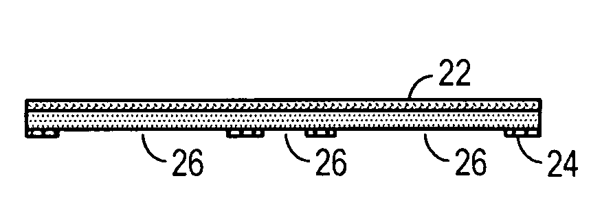
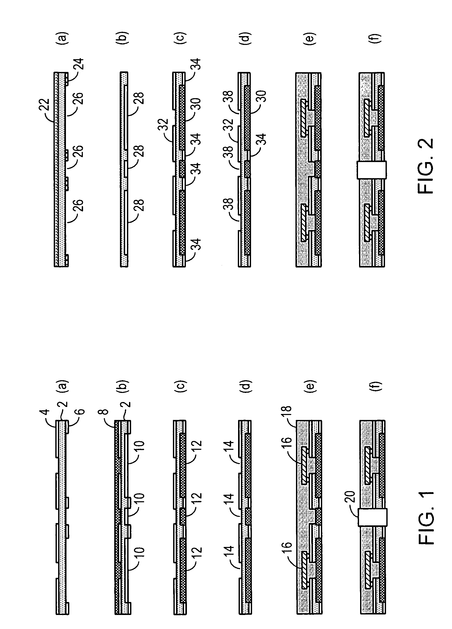
[0022]FIG. 1 illustrates one process incorporating the present invention. Here, in step a, a lead frame 2 is plated with an electrically conductor on the top 4 and the bottom 6. The top 4 is etched to form runs on the top that represent the final runs desired in the lead frame as a completed IC package. The bottom is etched 6 to form opening wide enough to accommodate later etching of cavities that separate multiple lead frames and provide a location for a pre-mold that will adequately support the lead from for later fabrication steps. In step b, the top is covered with a photo-resist 8 and the bottom is etched 10 away to form cavities that go half way through the lead frame 2.

[0023]In step c, the cavities 10 are then filled with a pre-mold material 12 that when solid form a strong assembly with the lead frame and the photo-resist 8 is removed. The pre-mold material may be any that are well known in the field.

[0024]Still viewing FIG. 1, in step d, the top is etched 14 completely thr...


PUM


Abstract

A lead frame with patterned conductive runs on the top surface to accept a wire bonded or flip-chip or COL configuration is disclosed. The top pattern is completed and the bottom is etched away creating cavities. The cavities are filled with a pre-mold material that lend structural support of the lead frame. The top is then etch through the lead frame to the pre-mold, except with the top conductive runs exist. In this manner the conductive runs are completed and isolated from each other so that the placement of the runs is flexible. The chips are mounted and the encapsulated and the lead frames are singulated. The pattern on the top and the bottom may be defined by first plated the patterns desired.

Description

BACKGROUND OF THE INVENTION[0001]1. Field of the Invention[0002]The present invention relates to designing lead frames for ICs (integrated circuits), and more particularly to partially or half etching techniques that provide a stable patterned lead frame that improves reliability for the resultant encapsulated packaged IC.[0003]2. Background Information[0004]Traditional lead frames for ICs accept wire bonds between the chip and the lead frame or accept the chip directly (flip chip or COL, chip on a lead). The chip is attached to the lead frame and encapsulated forming an assembly that is then separated from other assemblies. The lead frame completes the electrical connections from the chip to the outside world beyond the encapsulation.[0005]One continuing problem is the lead frame included etched leads that must be electrically isolated from all the other leads coming from an IC. This need results in very thin, flimsy leads that lack structural rigidity and difficult to hold in plac...

Claims


Application Information

Patent Timeline
IPC IPC(8): H01L23/495H01L21/00
CPCH01L21/4828H01L21/561H01L23/49558H01L23/49572H01L24/97H01L2224/97H01L2224/16245H01L2924/01082H01L2924/01013H01L2924/01006H01L2924/01005H01L2224/81H01L2924/14H01L2924/181H01L2924/00H01L2924/00012
Inventor LIM, LAY YEAPCHONG, DAVID
Owner SEMICON COMPONENTS IND LLC
Learn More