Card type information device and method for manufacturing same
- Summary
- Abstract
- Description
- Claims
- Application Information
AI Technical Summary
Benefits of technology
Problems solved by technology
Method used
Image
Examples
first exemplary embodiment
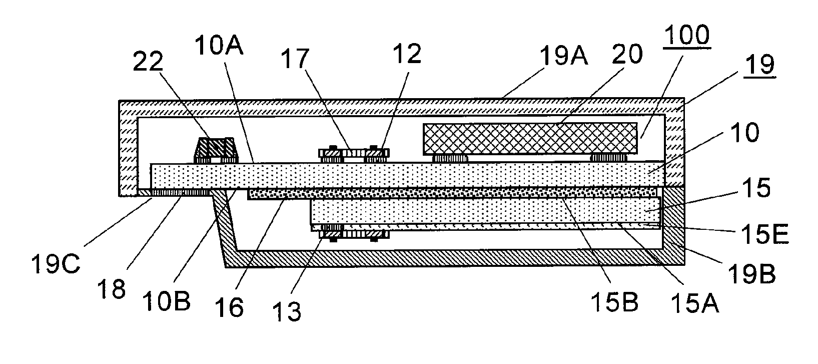
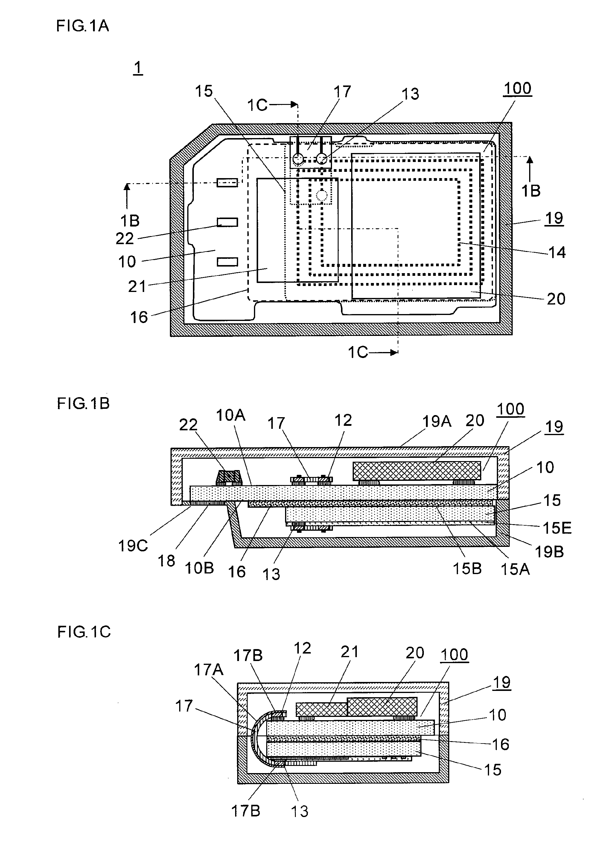
[0100]FIG. 1A shows a plan view schematically illustrates a structure of a card type information device (hereinafter referred to as SD memory card) in accordance with the first exemplary embodiment of the present invention. FIG. 1B shows a sectional view cut along line 1B-1B in FIG. 1A. FIG. 1C shows a sectional view cut along line 1C-1C in FIG. 1A. In FIG. 1A, an upper section of the housing is omitted in order to show the interior structure more clearly.
[0101]As shown in FIG. 1A, SD memory card 1 has outer dimensions of 24 mm×32 mm×2.1 mm specified by the industry standard and includes housing 19 made of a polymer alloy of polycarbonate and ABS resin. Housing 19 accommodates the following elements:[0102]wiring board 10 including a wiring pattern (not shown) having multiple electronic components, e.g. semiconductor memory elements, and control circuit elements mounted on first face 10A of wiring board 10, and antenna connecting electrode 12; and[0103]antenna board 15 of which first...
second exemplary embodiment
[0132]FIG. 6A shows a plan view schematically illustrates a structure of an SD memory card in accordance with the second exemplary embodiment of the present invention. FIG. 6B shows a schematic sectional view cut along line 6B-6B shown in FIG. 6A, and FIG. 6C shows a schematic sectional view cut along line 6C-6C shown in FIG. 6A. In FIG. 6A, an upper section of the housing is omitted in order to clearly show the interior structure. In FIG. 6A-FIG. 6C, similar elements to those in FIG. 1A-FIG. 1C have the same reference marks as those in FIG. 1A-FIG. 1C.
[0133]As shown in FIG. 6A-FIG. 6C, SD memory card 2 in accordance with the second exemplary embodiment differs from SD memory card 1 shown in FIG. 1A-FIG. 1C in the following point: Wiring board 10 and antenna board 15 of SD memory card 2 have a curved end face at least at a section where both wiring board 10 and antenna board 15 are coupled together through flexible wiring board 17.
[0134]To be more specific, as shown in FIG. 6C, SD m...
third exemplary embodiment
[0149]FIG. 10A shows a plan view schematically illustrates a structure of an SD memory card in accordance with the third exemplary embodiment of the present invention. FIG. 10B shows a schematic sectional view cut along line 10B-10B shown in FIG. 10A, and FIG. 10C shows a schematic sectional view cut along line 10C-10C shown in FIG. 10A. In FIG. 10A, an upper section of the housing is omitted in order to clearly show the interior structure. In FIG. 10A-FIG. 10C, similar elements to those in FIG. 1A-FIG. 1C have the same reference marks as those in FIG. 1A-FIG. 1C.
[0150]As shown in FIG. 10A-FIG. 10C, wiring board 10 differs from that shown in FIG. 1A-FIG. 1C in having no external connecting terminal, and the other structures remain unchanged from those in FIG. 1A-FIG. 1C. As shown in FIG. 10A-FIG. 10C, solid circuit module 400 of SD memory card 4 has no external connecting terminal at wiring board 40 for connecting to an external device through housing 49, so that no hole is needed t...
PUM
| Property | Measurement | Unit |
|---|---|---|
| Thickness | aaaaa | aaaaa |
| Flexibility | aaaaa | aaaaa |
| Magnetism | aaaaa | aaaaa |
Abstract
Description
Claims
Application Information
 - R&D
- Intellectual Property
- Life Sciences
- Materials
- Tech Scout
- Unparalleled Data Quality
- Higher Quality Content
- 60% Fewer Hallucinations
Browse by: Latest US Patents, China's latest patents, Technical Efficacy Thesaurus, Application Domain, Technology Topic, Popular Technical Reports.
© 2025 PatSnap. All rights reserved.Legal|Privacy policy|Modern Slavery Act Transparency Statement|Sitemap|About US| Contact US: help@patsnap.com


