
Semiconductor memory device and method for testing the same

a technology of semiconductor memory and memory device, which is applied in the direction of information storage, static storage, digital storage, etc., can solve the problem of taking a lot of time to test the mass-produced semiconductor memory device, and achieve the effect of reducing the number of data pads used in the test operation, improving the productivity of the semiconductor memory device, and increasing the burst length in the test operation

Inactive Publication Date: 2009-06-18
SK HYNIX INC
View PDF6 Cites 8 Cited by
  • Summary
  • Abstract
  • Description
  • Claims
  • Application Information

AI Technical Summary

Benefits of technology

[0013]Embodiments of the present invention are directed to providing a semiconductor memory device capable of sequentially connecting a plurality of banks to one data pad by increasing a burst length in testing a read operation and a write operation.
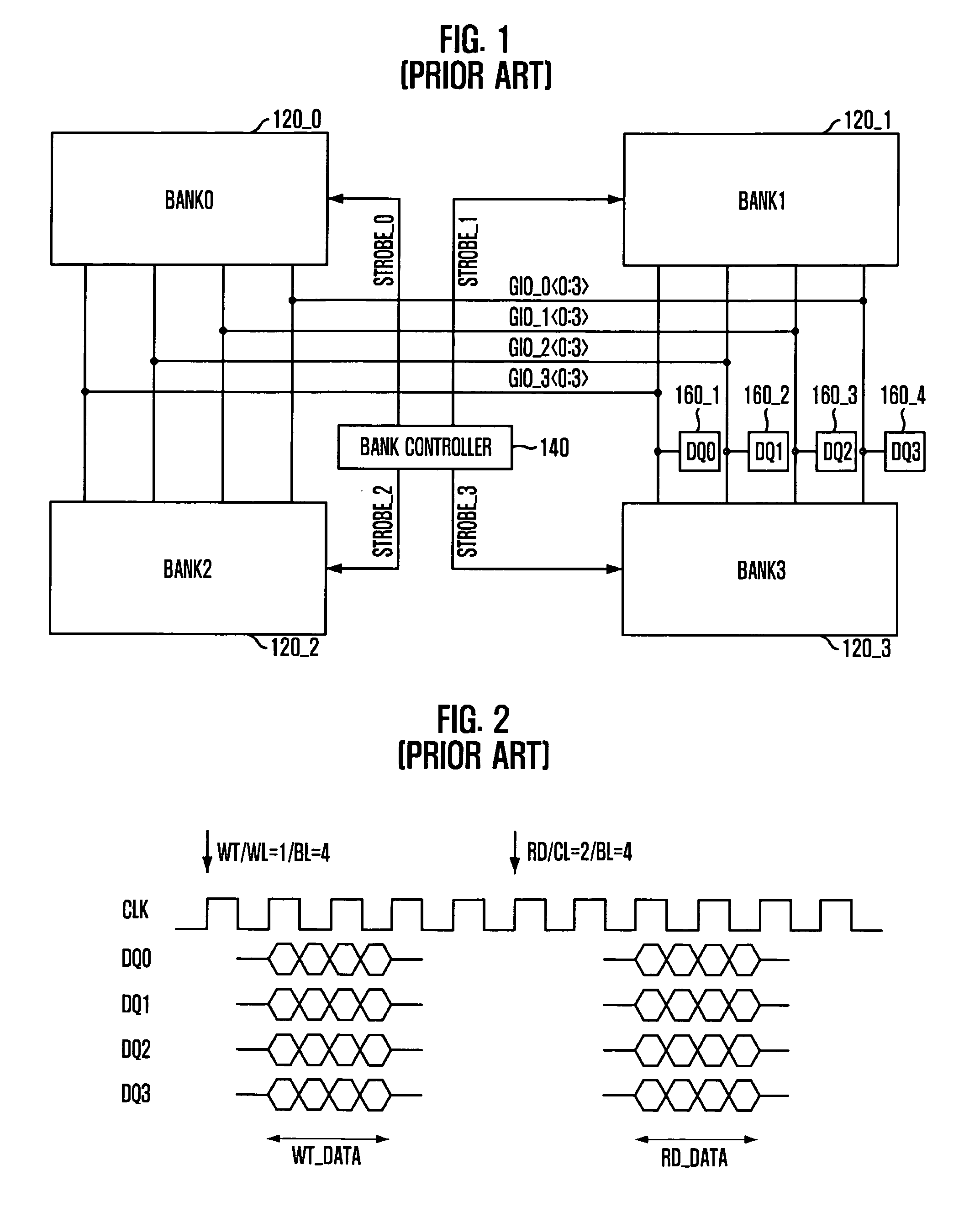
[0015]In accordance with the present invention, the number of data pads used in the test operation is reduced by increasing the burst length more than two times. A plurality of banks are sequentially selected and data are written to or read from the banks. In this way, the productivity of the semiconductor memory device is improved. The conventional test method is a parallel operation scheme to find internal defects by simultaneously writing and reading data to / from the banks. In this case, data are output through as many data pads as the minimal banks. In order to output the data, as many channels as the data pads must be allocated in the test apparatus. The conventional testing method has a disadvantage in that it takes a lot of time to test the mass-produced semiconductor memory devices. However, in accordance with the present invention, mass-produced semiconductor memory devices can be simultaneously tested while minimizing the number of channels to be allocated to the respective semiconductor memory devices. To this end, the burst length in the test operation is increased by the product of the number of data pads conventionally used and the predefined burst length. Therefore, a large quantity of semiconductor memory devices can be simultaneously tested by using one data pad.

Problems solved by technology

The conventional testing method has a disadvantage in that it takes a lot of time to test the mass-produced semiconductor memory devices.

Method used


Image

  • Semiconductor memory device and method for testing the same
  • Semiconductor memory device and method for testing the same
  • Semiconductor memory device and method for testing the same

Examples


Embodiment Construction

[0027]Hereinafter, a semiconductor memory device in accordance with the present invention will be described in detail with reference to the accompanying drawings.

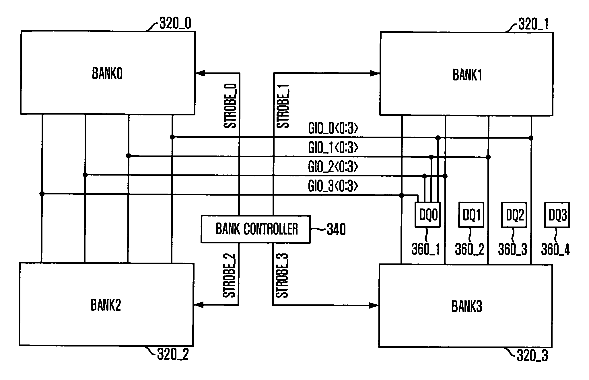
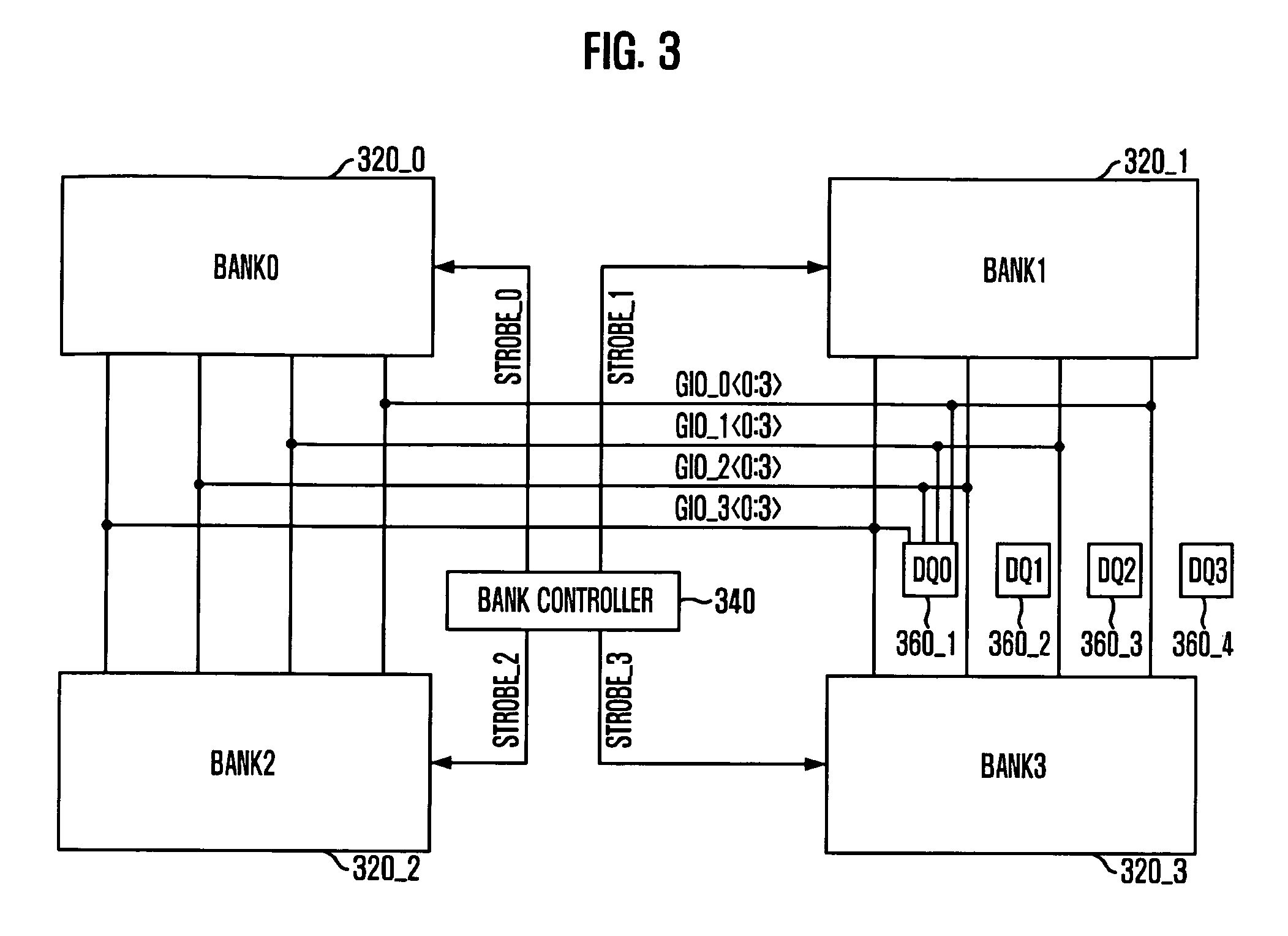
[0028]FIG. 3 is a block diagram of a semiconductor memory device in accordance with an embodiment of the present invention.

[0029]Referring to FIG. 3, the semiconductor memory device includes a plurality of banks 320_0 to 320_3, a bank controller 340 configured to enable the banks 320_0 to 320_3, and a plurality of data pads 360_1 to 360_4 through which data output from the banks 320_0 to 320_3 are transferred to the outside. Although FIG. 3 illustrates the data pads used to transfer data output from the banks in a test operation after the fabrication of the semiconductor memory device, more data pads are included in the semiconductor memory device.

[0030]When a read or write command is input to a semiconductor memory device in a test operation, the bank controller 340 sequentially activates bank select signals STROBE_0 to ST...


PUM


Abstract

Semiconductor memory device and method for testing the same includes a unit for characterized in that a burst length is increased in a test of a read operation and a write operation and a unit for connecting a plurality of banks to one data pad by sequentially and outputting the data.

Description

CROSS-REFERENCE TO RELATED APPLICATIONS[0001]The present invention claims priority of Korean patent application number 10-2007-0128812, filed on Dec. 12, 2007, which is incorporated by reference in its entirety.BACKGROUND OF THE INVENTION[0002]The present invention relates to a semiconductor memory device, and more particularly, to a semiconductor memory device capable of reducing additional circuits required in a test operation after a large-capacity semiconductor memory device is fabricated.[0003]In a system with a variety of semiconductor devices, a semiconductor memory device serves as a data storage. The semiconductor memory device outputs data corresponding to addresses received from a data processor, e.g., a central processing unit (CPU), or stores data received from the data processor into memory cells selected by addresses.[0004]As the operating speed of the system increases and semiconductor integrated circuit technologies are advanced, semiconductor memory devices are req...

Claims


Application Information

Patent Timeline
Patent Type & Authority Applications(United States)
IPC IPC(8): G11C29/00
CPCG11C29/1201G11C2029/1804G11C29/48G11C29/26G11C7/10G11C29/00
Inventor KWEAN, KI-CHANG
Owner SK HYNIX INC
Learn More