
Flat screen detector

Inactive Publication Date: 2009-06-04
SIEMENS AG
View PDF3 Cites 6 Cited by
  • Summary
  • Abstract
  • Description
  • Claims
  • Application Information

AI Technical Summary

Benefits of technology

[0010]An object of the invention is to provide a flat panel detector for which manufacture is simplified even given the use of different substrates for the transistor matrix.
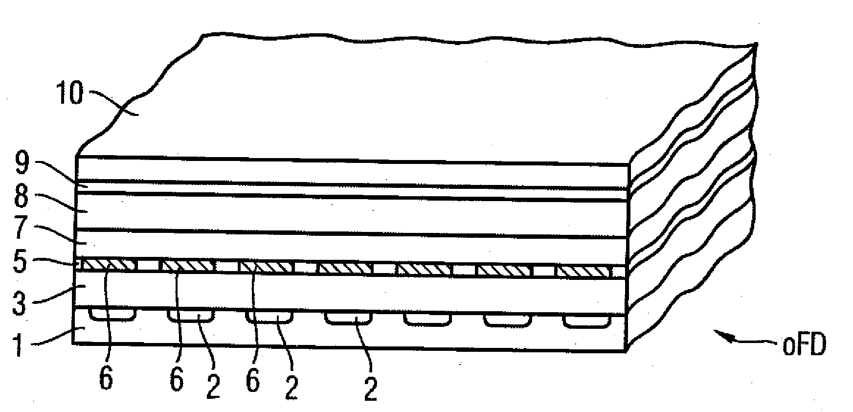
[0012]The basis of the inventive flat panel detector is thus to not build the photodetector directly on the substrate with the transistor matrix, but rather to initially provide the substrate with the passivation layer and to build the photodetector on this passivation layer. The photodetector is spatially separated from the substrate via the passivation layer. It is thus possible for the photodetector to be arranged vertically above the individual transistors, so the surface of the photodetector is enlarged. The filling factor of the photodetector thus can be increased.
[0015]The passivation layer is preferably applied on the substrate by means of printing techniques. The inventive flat panel detector can thereby be manufactured in a particularly cost-effective manner.

Problems solved by technology

One disadvantage of this embodiment is that the structure of the laminar photodetector must be adapted to the structure of the substrate, which is determined by the transistors of the transistor matrix.

Method used


Image

  • Flat screen detector
  • Flat screen detector
  • Flat screen detector

Examples


Embodiment Construction

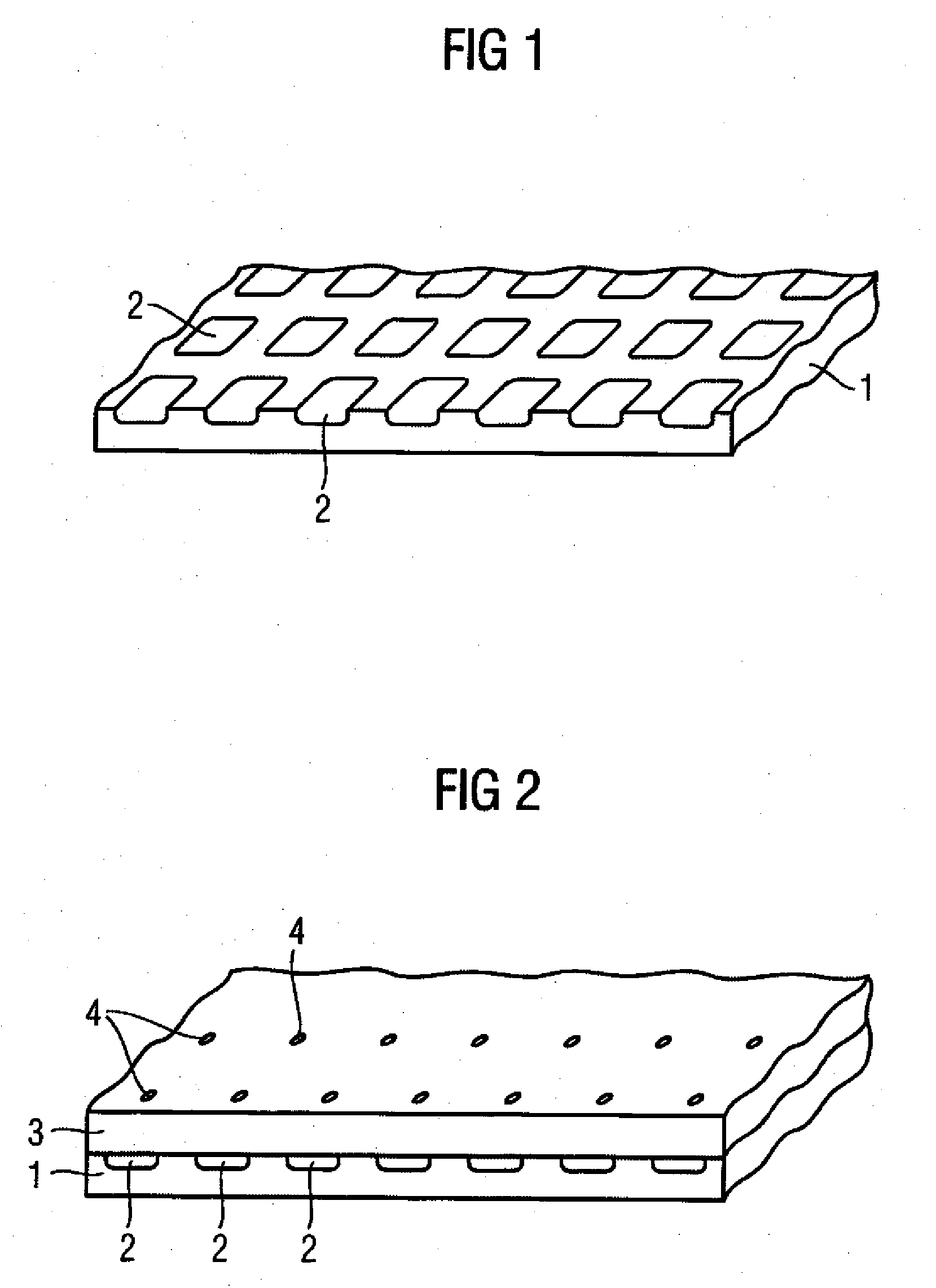
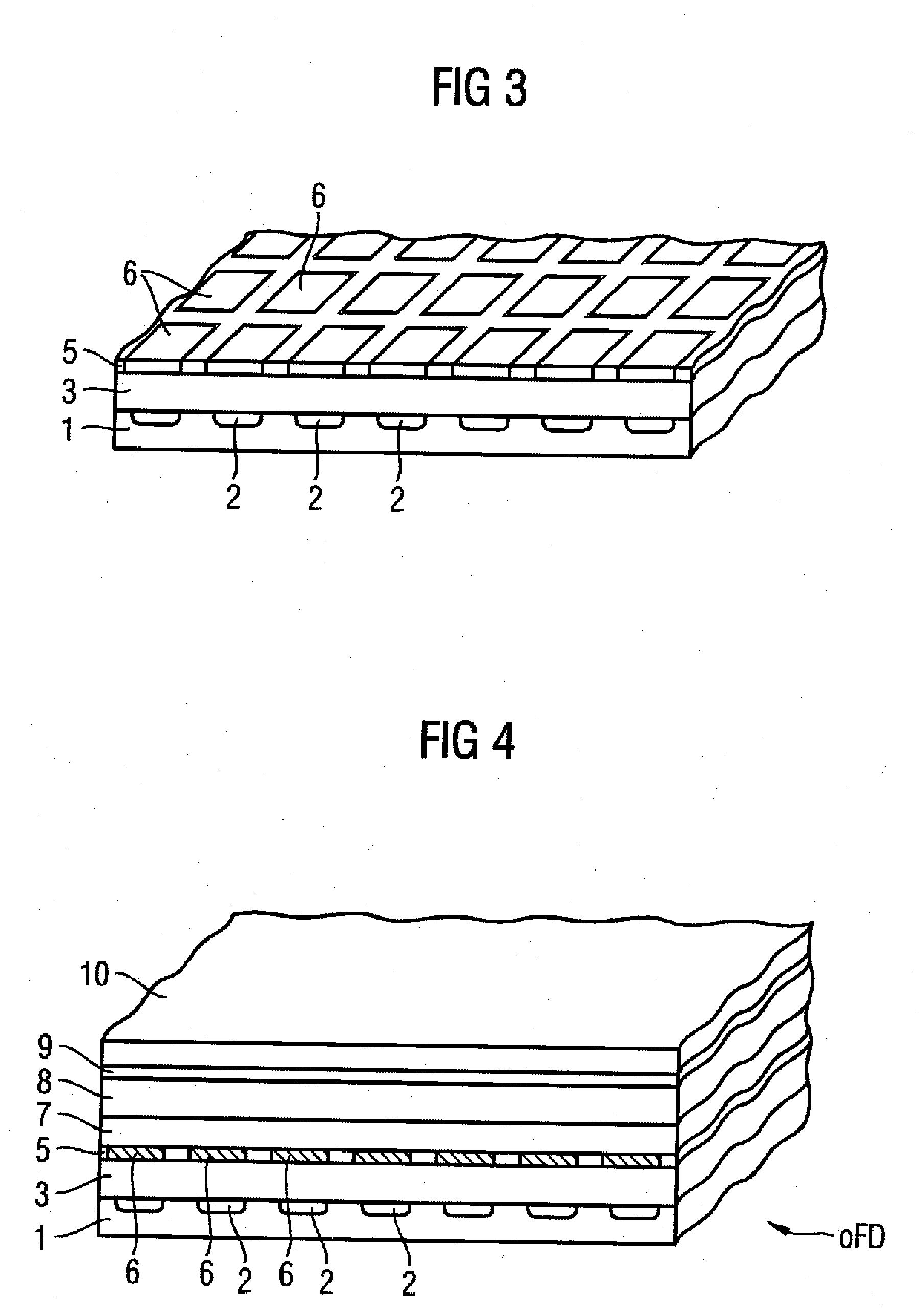
[0021]FIGS. 1 through 4 illustrate the manufacture of an inventive flat panel detector with an organic photodetector (oPD).

[0022]FIG. 1 shows in section a substrate 1 with a transistor matrix comprising a plurality of transistors 2. In the case of the present exemplary embodiment the individual transistors 2 are a-Si FETs that have been produced by means of thin-film technology. Each of the transistors 2 is associated with a pixel of an image to be acquired with the flat panel detector.

[0023]A passivation layer 3 (shown in FIG. 2) is subsequently applied on the substrate 1. In the case of the present exemplary embodiment the passivation layer 3 (which comprises a significantly electrically-insulating material) was applied on the substrate 1 by means of known printing techniques, subsequently structured (as shown in FIG. 2) by means of photo-techniques and finally planarized. Via the structuring the passivation layer 3 receives vias 4 (thus vertical holes) that are filled with an ele...


PUM


Abstract

A flat screen detector has a substrate with a transistor matrix thereon, a photodetector, and a passivation layer. The photodetector includes a structured first electrode including a number of sub-electrodes, a second electrode, and a photoactive layer between the first and second electrodes. The passivation layer is located between the substrate having the transistor matrix and the first electrode.

Description

BACKGROUND OF THE INVENTION[0001]1. Field of the Invention[0002]The invention concerns a flat panel detector of the type having a substrate carrying a transistor matrix and a photodetector.[0003]2. Description of the Prior Art[0004]With a flat panel detector, light striking the flat panel detector is transduced into electrical signals that can be converted into an image data set with a suitable evaluation device. The image associated with the image data set can be visualized with a viewing apparatus.[0005]Current flat panel detectors are a combination of a pixelated photodetector and a transistor matrix.[0006]The pixelated photodetector essentially has two electrodes and a semiconductor layer arranged between the two electrodes. One of the electrodes is structured such that it comprises a plurality of sub-electrodes insulated from one another that are respectively associated with a pixel of an image to be acquired with the flat panel detector.[0007]For acquiring an image with the fl...

Claims


Application Information

Patent Timeline
IPC IPC(8): H01L31/0256H01L31/0224
CPCB82Y10/00H01L27/14665H01L51/0096H01L51/0036H01L51/0046H01L27/307H10K39/32H10K85/113H10K85/211H10K77/10
Inventor BRABEC, CHRISTOPHWITTMANN, GEORG
Owner SIEMENS AG
Learn More