Method and apparatus for residue detection on a polished wafer

a technology of residue detection and polishing, applied in the direction of electrical equipment, material analysis, instruments, etc., can solve the problems of affecting the quality of the final product, not removing the entire metal layer, and leaving residue on the processed wafer

Inactive Publication Date: 2009-05-28
MAY HIGH TECH SOLUTIONS
View PDF15 Cites 36 Cited by
  • Summary
  • Abstract
  • Description
  • Claims
  • Application Information

AI Technical Summary

Benefits of technology

[0025]In accordance with the present invention there is provided an automatic optical inspection tool of an apparatus for residue detection on polished wafers, comprising an inspection tool, an illumination source, capable of instantaneous entire wafer surface illumination, colour digital camera, encompassing the entire wafers surface without eclipse, in a duple of consecutive, properly delayed imaging shots and providing appropriate image resolution for tiny residue detection, computation means, implementing image processing and manipulation algori...

Problems solved by technology

It often occurs, however, that not the entire metal layer is removed, due mostly to the process control impairments, such as pads fractional damage, thereby leaving a residue on the processed wafer.
The presence of a residue might impair the quality of the final product.
The yield and productivity are adversely affected if the residue presence is not detected on time.
The prior art indirect end-point polishing on-process technique implemented in numerous manufacturers' polishing tools for process control doesn't prevent processing residue events and the inspection for remains becomes a necessity.
This process is time-consuming and labor-intensive, human error prone and its off-process implementation interferes with the manufacture process flow, causing time, productivity and production floor area losses.
They have limitations in heavily patterned wafers inspection, are off-process implemented and their inspection throughput rate is low.
Alternatively, complicated and bulky multi-beam parallel illumination a...

Method used


Image

  • Method and apparatus for residue detection on a polished wafer
  • Method and apparatus for residue detection on a polished wafer
  • Method and apparatus for residue detection on a polished wafer

Examples


Embodiment Construction

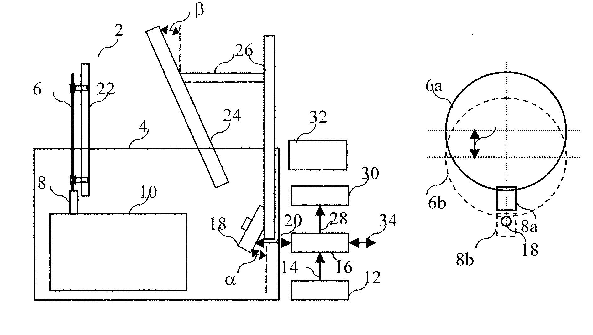
[0047]FIGS. 1a and 1b are schematic drawings of side (a) and front (b) projections of the present invention apparatus arrangement 2, mounted on a parent tool 4. The static FIG. 1a presentation corresponds to a certain moment in parent tool 4 robot dynamics, when a wafer 6 settles on download lifter 8 in its uppermost position, before descending to the output cassette 10. The electronic section 12 of the parent tool 4 then produces a trigger signal, which is fed through link 14 to the apparatus computer 16. The computer in turn triggers a camera 18 through link 20 after a necessary delay, when the utmost opening of robots arm's wafer grip 22 causes no line-of-sight obstruction from camera 18 to wafer 6. The inspection tool illumination source 24 and camera 18 are mounted on supporting structure 26, which is clamped to the chassis of the parent tool 4. The illumination source 24 and camera 18 are both inclined by about 30° angles α, β, respectively, relative to vertical (in opposite d...


PUM


Abstract

There is provided an automatic optical inspection tool of an apparatus for residue detection on polished wafers, including an inspection tool, an illumination source, capable of instantaneous entire wafer surface illumination, colour digital camera, encompassing the entire wafers surface without eclipse, in a duple of consecutive, properly delayed imaging shots and providing appropriate image resolution for tiny residue detection, computation means, implementing image processing and manipulation algorithms to enable residue detection and characterization, logic and command operations execution and camera control, the computation means accumulating an on-line created wafer images and wafer residue defects data base, the computation means providing for inspection tool worthiness monitoring, wafer handling and transportation means. A method of automatic optical self-contained inspection for pattern wafers' polishing residue detection is also provided.

Description

CROSS REFERENCE TO RELATED APPLICATIONS[0001]This application is a National Stage of International Application No. PCT / IL2005 / 001110, filed Oct. 26, 2005, and which claims the benefit of U.S. Provisional Patent Application No. 60 / 622,443, filed Oct. 26, 2004. The disclosure of the above applications are incorporated herein by reference.FIELD OF THE INVENTION[0002]The present invention pertains in general to the semiconductor integrated circuits device manufacturing. More specifically, the present invention relates to wafers processing quality inspection and, in particular, to a method and apparatus for polishing residue detection and characterization, and polishing operation working order assessment.BACKGROUND OF THE INVENTION[0003]Chemical-mechanical polishing (CMP) is a well-known process in the semiconductors manufacturing industry. It removes and planarizes metal, alloy and dielectric material layers deposited on wafer's surface. CMP typically involves mechanical polishing of th...

Claims


Application Information

Patent Timeline
IPC IPC(8): G06K9/00
CPCG01N21/93H01L21/67242G01N21/9501G01N21/94
Inventor BARKOL, ARIEGUTMAN, MOSHEFIREAIZEN, HAIM MOSHEPEISACH, AVIVAROSENBERG, MOSHE
Owner MAY HIGH TECH SOLUTIONS
Why Eureka
Try Eureka