Dual-frequency matching circuit

a matching circuit and dual-frequency technology, applied in the direction of waveguide type devices, antenna details, antennas, etc., can solve the problems of difficult to stabilize the matching property with respect, difficult for a normal single-frequency matching circuit to carry out flexible matching and adjustment on both of these two frequency bands, and difficult to realize good antenna properties on multiple desired frequency bands

Inactive Publication Date: 2009-05-14
PANASONIC CORP
View PDF5 Cites 13 Cited by
  • Summary
  • Abstract
  • Description
  • Claims
  • Application Information

AI Technical Summary

Benefits of technology

[0019]The dual-frequency matching circuit of the present invention can resolve the two major technological issues (i.e., loss reduction and stabilization of matching property).

Problems solved by technology

In actually developing a mobile terminal, however, it is extremely difficult to realize good antenna properties on multiple desired frequency bands just by optimizing the configuration of the antenna.
However, these two frequency bands are so far apart from each other that it is difficult for a normal single-frequency matching circuit to carry out flexible matching and adjustment on both of these two frequency bands.
Firstly, it is difficult to reduce the loss caused by the dual-frequency matching circuit. To improve the quality of cellphone services, the transmission and receiving properties of mobile terminals must be improved. The transmission and receiving properties are improved mainly by reducing the transmission loss between the antenna and the RF circuit. That is why the loss to be caused by the dual-frequency matching circuit inserted there is preferably as little as possible. The conventional configuration, however, needs too many elements (including inductors and capacitors) and must use a number of resonant circuits, and therefore, is a problem as far as loss reduction is concerned.
Another problem is that it is difficult to stabilize the matching property with respect to the variation in the impedance of the load 101.

Method used


Image

  • Dual-frequency matching circuit
  • Dual-frequency matching circuit
  • Dual-frequency matching circuit

Examples


embodiment

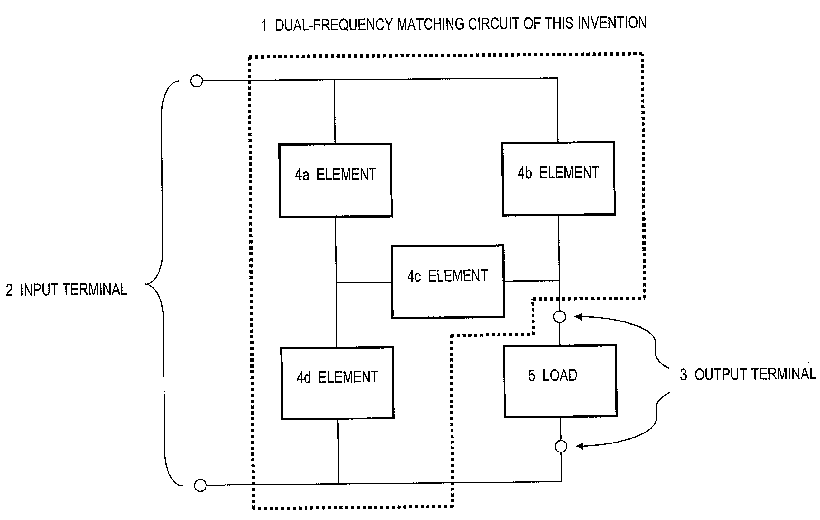
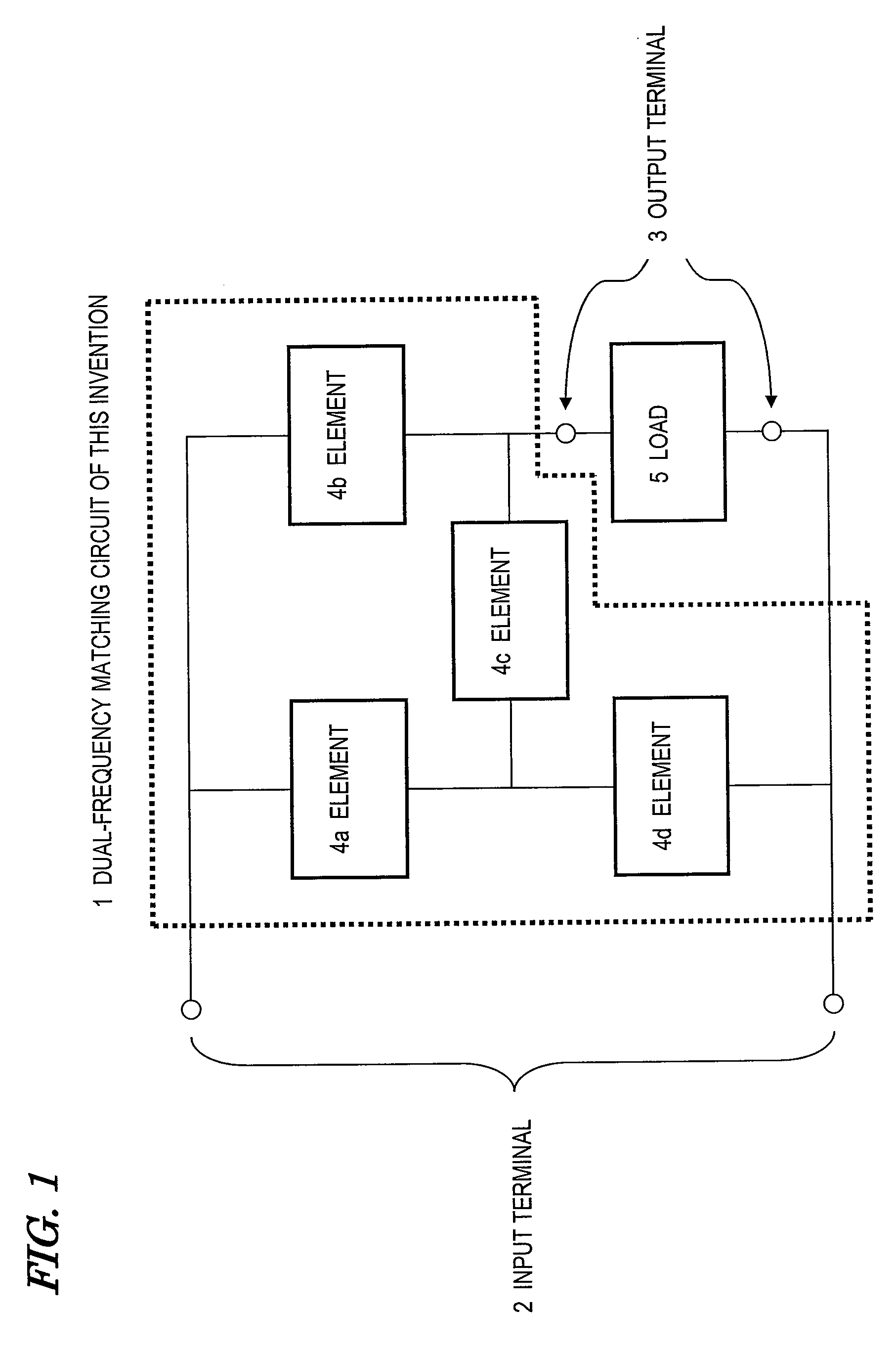
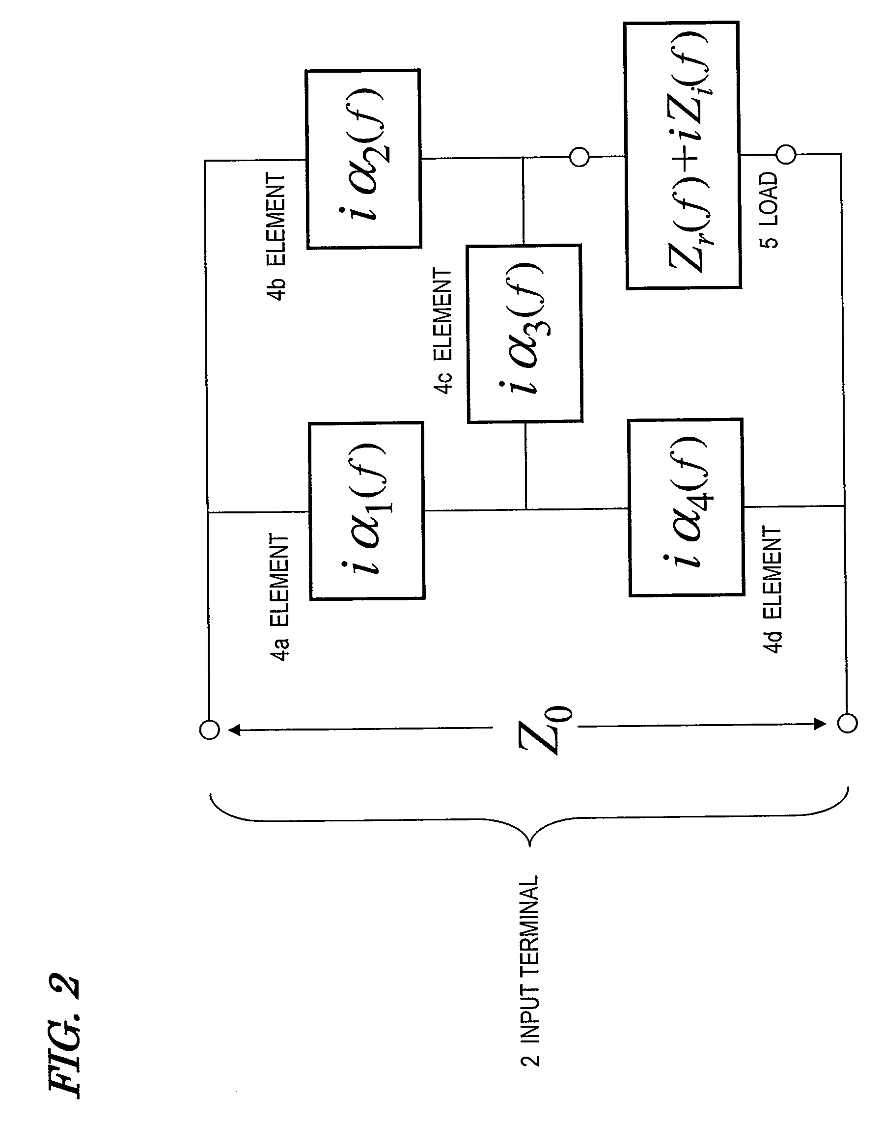
[0044]FIG. 1 is a circuit block diagram illustrating a circuit configuration for a dual-frequency matching circuit as a preferred embodiment of the present invention. As shown in FIG. 1, the dual-frequency matching circuit 1 of this preferred embodiment includes input terminals 2 consisting of first and second input terminals 2a and 2b and output terminals 3 consisting of first and second output terminals 3a and 3b. An RF circuit (not shown) is connected to the input terminals 2, while a load 5 is connected to the output terminals 3.

[0045]The dual-frequency matching circuit 1 of this preferred embodiment includes four elements 4a, 4b, 4c and 4d, which are lumped constant elements and each of which is either an inductor or a capacitor. The types of these elements 4a, 4b, 4c and 4d, which should be either inductors or capacitors, and the specific values of their respective element constants are determined unequivocally by the impedance value of the load 5 that has been defined in adva...

specific example 1

[0059]Hereinafter, a specific example of a dual-frequency matching circuit according to the present invention will be described. The basic configuration of this specific example is the same as the configuration of the preferred embodiment shown in FIG. 1.

[0060]FIG. 4 is a perspective view showing the dimensions of an analytical model for a mobile terminal with an antenna as a specific example of the present invention. Specifically, FIG. 4A is a perspective view showing the overall dimensions of the analytical model and FIG. 4B is a perspective view showing the detailed dimensions of the antenna portion thereof. In FIG. 4, the entire analytical model is made of a metallic plate with a thickness of 100 μm and a conductivity of 4.9×10̂7 Sie / m.

[0061]As shown in FIG. 4A, the antenna 6 is an inverted F antenna formed by folding the metallic plate and is connected to the top end of a metallic box with dimensions of 40 mm×85 mm×5 mm, which represents a model of the housing 7 of a mobile ter...

specific example 2

[0082]Hereinafter, another specific example of a dual-frequency matching circuit according to the present invention will be described.

[0083]The frequency bands that are already utilized currently and the ones that will be exploited in the near future can be roughly classified into the three frequency bands, namely, a low frequency band in a 0.45 GHz range, an intermediate frequency band in 0.8 GHz, 0.85 GHz and 0.9 GHz ranges, and a radio frequency band in 1.5 GHz, 1.7 GHz, 1.8 GHz, 1.9 GHz and 2.0 GHz ranges. Among other things, the intermediate and radio frequency bands are in particularly high demand for common use. For that reason, in this specific example, a representative frequency of 0.85 GHz is selected from the intermediate frequency band and three representative frequencies of 1.55 GHz, 1.7 GHz and 2.05 GHz are selected from the radio frequency band to design an antenna first.

[0084]These frequencies are selected because all the other frequency bands are asymptotic to one o...


PUM


Abstract

The connection topology of input terminals 2, elements 4a, 4b, 4c and 4d and load 5 is designed similarly to a so-called “seven-segment display”, which is often used to display numerals on an electronic calculator or a digital watch. More specifically, suppose in the three horizontally running segments, the top and bottom segments are associated with the input terminals 2 and the load 5 is allocated to one of the four vertically running segments. Then, the three other vertical segments and the other horizontal segment are associated with the elements 4a, 4b, 4c and 4d, which are an inductor with an inductance of 5.119 nH, a capacitor with a capacitance of 1.370 pF, an inductor with an inductance of 8.360 nH and a capacitor with a capacitance of 5.942 pF, respectively. By adopting this circuit configuration, the total number of elements can be reduced to four and the loss can be reduced significantly. In addition, since the resonant circuits can be eliminated and the size of the ladder circuit can be reduced, impedance matching is achieved with a high degree of stability.

Description

[0001]This is a continuation of International Application No. PCT / JP2008 / 002349, with an international filing date of Aug. 28, 2008, which claims priority of Japanese Patent Application No. 2007-222393, filed on Aug. 29, 2007, the contents of which are hereby incorporated by reference.BACKGROUND OF THE INVENTION[0002]1. Field of the Invention[0003]The present invention relates to a dual-frequency impedance matching circuit to be inserted between an antenna and an RF circuit in a mobile terminal in order to carry out impedance matching between the antenna and the RF circuit in two arbitrary frequency bands.[0004]2. Description of the Related Art[0005]As cellphone services have become amazingly popular nowadays, there are increasing demands for an even higher degree of mobility and even more versatile telecommunications services. To meet such demands, it is now one of the major technological objects to develop a mobile terminal that has an even smaller size and yet can use multiple te...

Claims


Application Information

Patent Timeline
Patent Type & Authority Applications(United States)
IPC IPC(8): H03H7/38H01Q1/50H01Q5/10
CPCH04B1/0458H03H7/38
Inventor SANGAWA, USHIO
Owner PANASONIC CORP
Why Eureka
Try Eureka