Device for measuring an aerial image produced by an optical lithography system

an optical lithography system and aerial image technology, applied in the field of aerial image measurement, can solve the problems of inaccurate aerial image profiles created from those measurements, affecting the measurement of aerial images, and affecting the imaging performance of optical lithography systems, so as to reduce or substantially eliminate the dependence on incident angle and polarization sta

Inactive Publication Date: 2009-05-07
CANON KK
View PDF3 Cites 0 Cited by
  • Summary
  • Abstract
  • Description
  • Claims
  • Application Information

AI Technical Summary

Benefits of technology

[0012]According to one aspect of the invention, a wavelength conversion element is provided in an aerial image measuring device, so as to reduce or substantially eliminate dependence on incident angle and polarization state. More particularly, the aerial image measuring device includes a substrate in which there are photo-luminescent nanoparticles that isotropically emit a photo-luminescent wavelength in response to an illuminated wavelength of the aerial image, a filter that blocks the illuminated wavelength and is transparent to the photo-luminescent wavelength, and a light detector that is sensitive to light of the photo-luminescent wavelength. The substrate is transparent to light of both the illuminated and the photo-luminescent wavelength, and the aerial image passes through the substrate and illuminates the nanoparticles. The photoluminescent light emitted by the nanoparticles passes through the filter and enters the light detector, which measures the aerial image. The aerial image is scanned by the aerial image measuring device.
[0014]Using this image measuring device to measure an aerial image is likely to result in more accurate aerial image profiles because the nanoparticles respond to an incident light beam isotropically, independent of the incident angle and the incident polarization state. Because of the nanoparticle's isotropic emission, and reinforced in nanoparticles having a spherical shape, the photo-luminescent light is emitted uniformly into the surrounding space. Thus, the portion of this photo-luminescent light detected by the light detector is not significantly affected by the incident angle or polarization state of the incident light from the aerial image. Furthermore, because of the nanoparticle's small size, the measuring device may provide a high resolution capable of measuring small structures in an aerial image. Thus, the image measuring device may result in more accurate aerial image profiles.
[0016]The image measuring device can have at least one light-blocking layer that blocks the illuminated wavelength, and the light-blocking layer can be arranged to reduce an amount of light of the illuminated wavelength that reaches the filter. The image measuring device can have a lens arranged to guide light of the photo-luminescent wavelength to the light detector. At least one reflecting surface can be arranged to deflect light of the photo-luminescent wavelength to the light detector. By virtue of the light blocking layer, lens, and reflecting surfaces, a more accurate aerial image profile can be attained.

Problems solved by technology

A limitation of aerial image measuring devices (e.g., 200 of FIG. 2) noticed by the inventor herein is that aerial image measurements may depend upon the incident angle and polarization state of beams projected onto the measuring device.
Because an aerial image is created by the interference of these beams, changes in the properties of these beams may affect measurements of the aerial image.
Because typical aerial image measuring devices (e.g., 200) may not accurately measure an aerial image for the foregoing reasons, aerial image profiles created from those measurements may not be accurate.
Thus, these aerial images profiles may not accurately represent the imaging performance of an optical lithography system (e.g., 1).

Method used


Image

  • Device for measuring an aerial image produced by an optical lithography system
  • Device for measuring an aerial image produced by an optical lithography system
  • Device for measuring an aerial image produced by an optical lithography system

Examples


Embodiment Construction

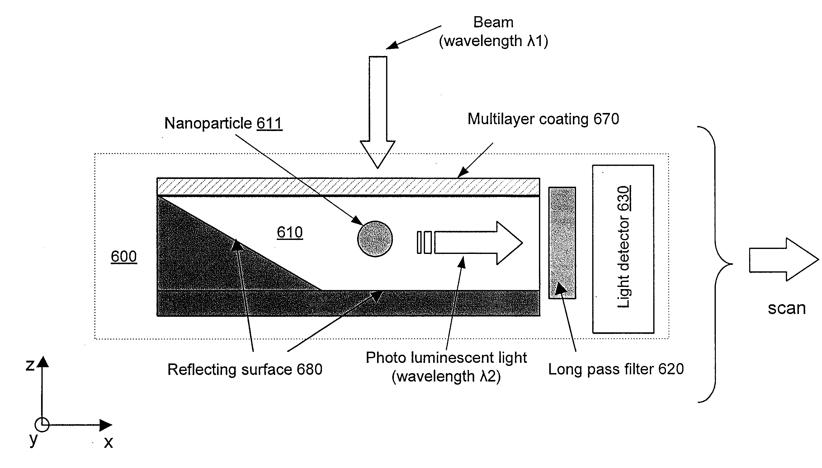
[0036]FIGS. 5A shows the configuration of an aerial image measuring device 500 according to embodiments of the invention. Aerial image measuring device 500 includes a substrate 510, a light detector 530, and a filter 520 positioned between substrate 510 and light detector 530, as illustrated in FIG. 5A.

[0037]Nanoparticles 511 are embedded in substrate 510, and arranged in a column along the Y-axis, as shown in FIG. 5B (which depicts a top view of measuring device 500 of FIG. 5A). Nanoparticles 511 are arranged within substrate 510 in a manner such that individual nanoparticles 511 do not touch each other.

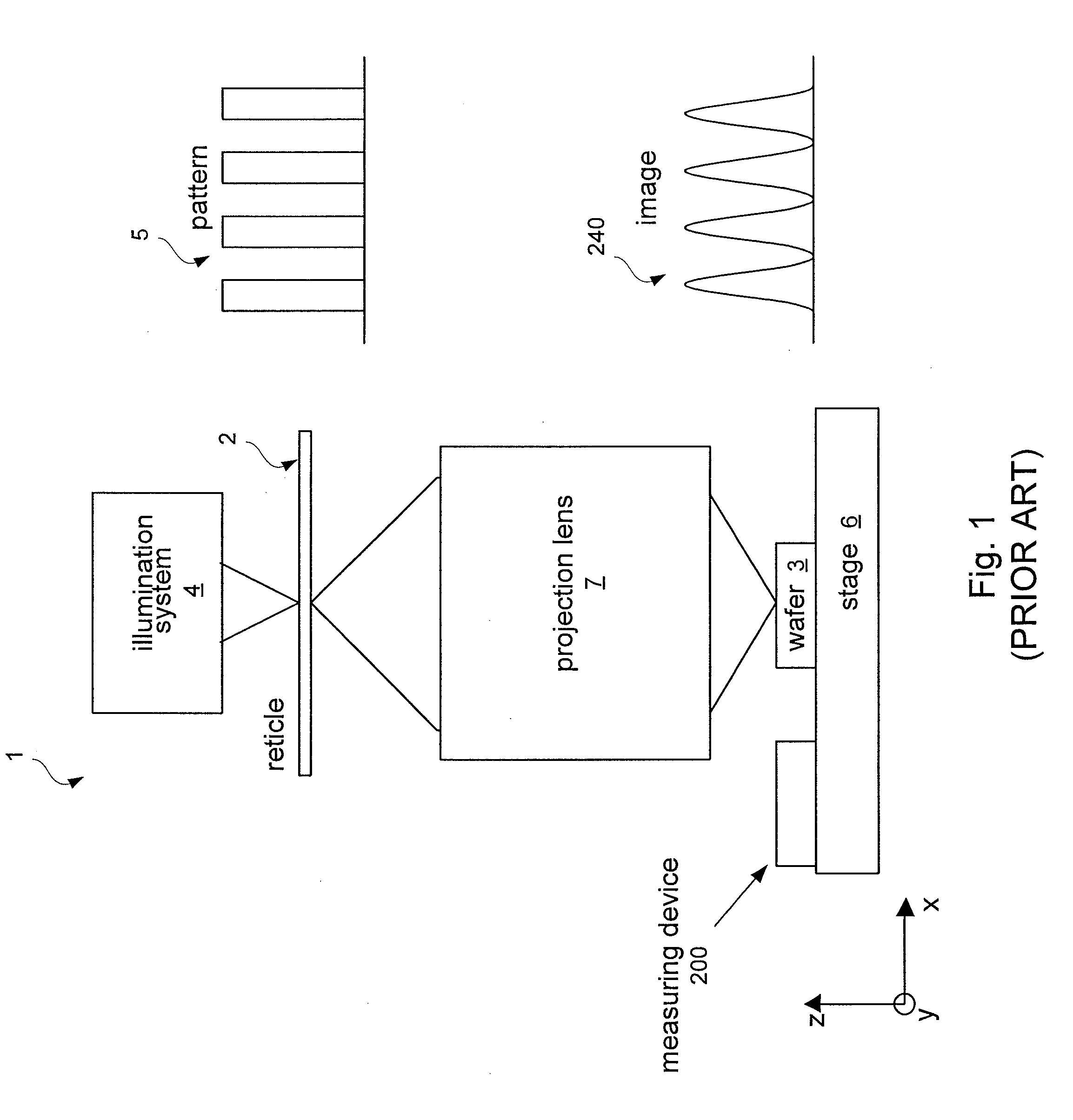
[0038]Nanoparticles 511 are between 5 nm and 20 nm in diameter, and are smaller than both the illuminated wavelength λ1 and a feature size of aerial image 540. In optical lithography systems, such as the system shown in FIG. 1, that use ArF excimer lasers for illumination, the illuminated wavelength λ1 is typically 193 nm.

[0039]Nanoparticles 511 can include, for example, substantial...


PUM


Abstract

An image measuring device that measures an aerial image, with relatively small or no dependence on the incident angle and polarization state of the beams projected onto the measuring device. The aerial image measuring device includes a substrate in which there are photo-luminescent nanoparticles that isotropically emit a photo-luminescent wavelength in response to an illuminated wavelength of the aerial image, a filter that blocks the illuminated wavelength and is transparent to the photo-luminescent wavelength, and a light detector that is sensitive to light of the photo-luminescent wavelength. The substrate is transparent to light of both the illuminated and the photo-luminescent wavelength, and the aerial image passes through the substrate and illuminates the nanoparticles. The photoluminescent light emitted by the nanoparticles passes through the filter and enters the light detector, which measures the aerial image. The aerial image is scanned by the aerial image measuring device

Description

BACKGROUND OF THE INVENTION[0001]1. Field of the Invention[0002]The invention relates to aerial image measurement, and more particularly relates to measuring an aerial image produced by an optical lithography system.[0003]2. Description of the Related Art[0004]FIG. 1 shows the configuration of a typical optical lithography system 1 used for the manufacturing of semiconductor devices. A pattern 5 on reticle 2 is illuminated by illumination system 4, thereby creating an image 240 of pattern 5. Projection lens 7 projects image 240 of pattern 5 onto wafer 3 (positioned on wafer stage 6).[0005]To evaluate the effects of lens aberrations, illumination conditions, and other factors that affect the imaging performance of the lithography system 1, aerial image 240 is measured by aerial imaging measuring device 200 (positioned on wafer stage 6). By moving wafer stage 6 along the X and / or Y direction, aerial image 240 can be measured by measuring device 200.[0006]FIG. 2 shows the basic configu...

Claims


Application Information

Patent Timeline
Patent Type & Authority Applications(United States)
IPC IPC(8): G06K9/00B05D1/12
CPCG03F7/70575G03F7/70958G03F7/7085G03F7/70666
Inventor UNNO, YASUYUKI
Owner CANON KK
Why Eureka
Try Eureka