
Stress-induced bandgap-shifted semiconductor photoelectrolytic/photocatalytic/photovoltaic surface and method for making same

a technology of photocatalytic and semiconductor, applied in the direction of catalyst activation/preparation, chemical/physical processes, disinfection, etc., can solve the problems of pollution of land and oceans, and well-known carbon-based energy problems, and achieve high stress in titania, better matched, and high efficiency

Inactive Publication Date: 2009-04-30
NANOPTEK CORP
View PDF12 Cites 15 Cited by
  • Summary
  • Abstract
  • Description
  • Claims
  • Application Information

AI Technical Summary

Benefits of technology

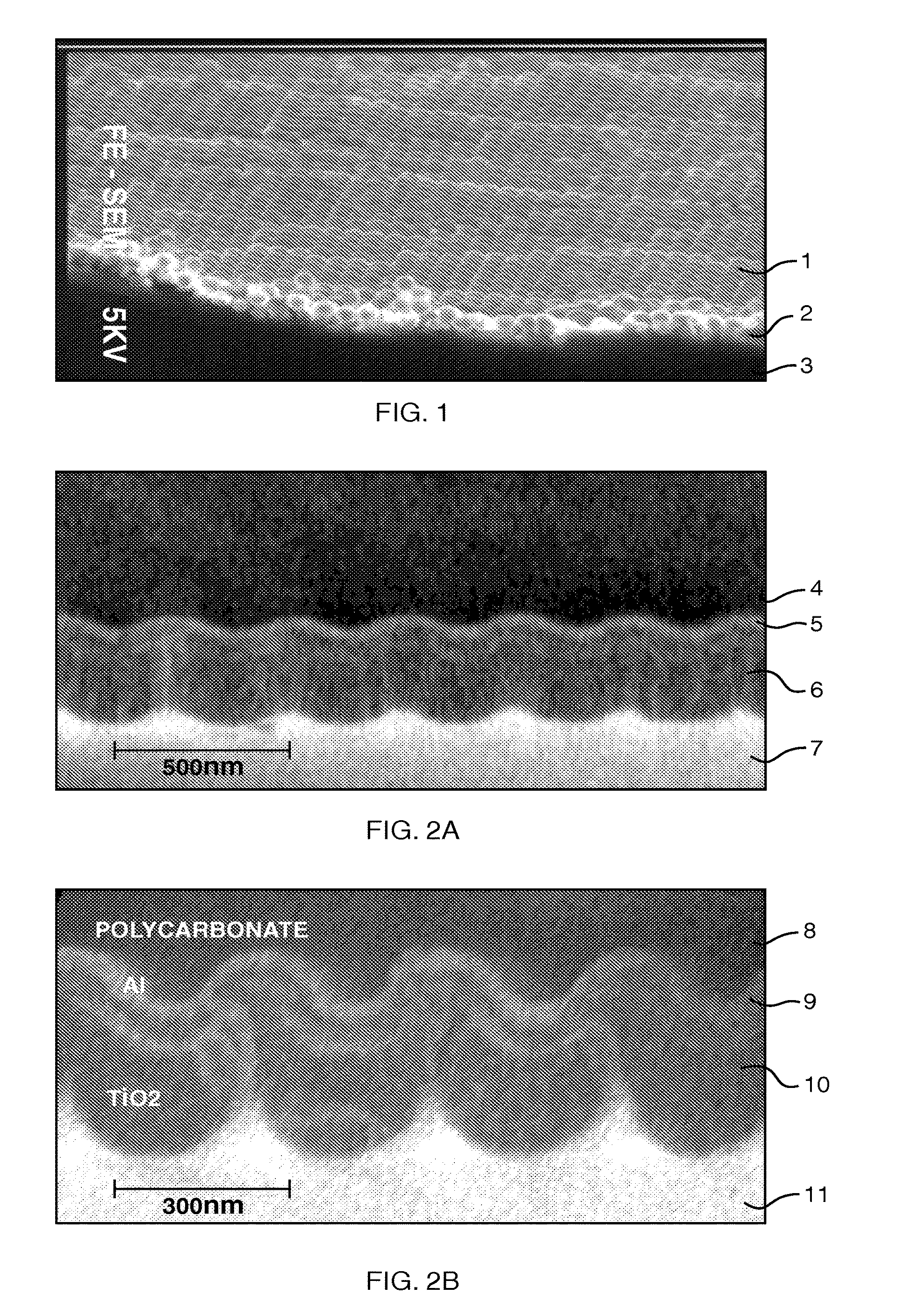
[0031]One would like a semiconductor photocatalyst with a bandgap that is better matched to the solar spectrum and / or artificial illumination for higher efficiency or even to work at all. In this invention, the bandgap of the known chemically-inert photocatalyst titania (TiO2) is shifted and broadened to be active at wavelengths more prevalent in sunlight and artificial light by inducing and managing sufficiently high stress in titania by vacuum coating a thin film of titania onto a substrate, preferably of a different Young's modulus, with bending undulations on the surface of a spatial radius similar to the film thickness. The undulated coating also serves to self-focus and concentrate the incident light required for the process, increase photocatalytic surface area, and prevent delamination of the film from the substrate. The electrical activity so induced in the band-shifted titania subsequently by visible light is applied to photoelectrolysis (hydrogen production from water and light), photovoltaics (electrical power from sunlight), photocatalytic disinfection and detoxification, point-of-use photoelectrolysis for use in internal combustion engines, for example, and stress-induced tunable bandgap components for communications. In addition, the same stress-induced thin film bandgap shifting works with other semiconductors such as amorphous silicon, and with similar benefits.
[0032]Accordingly, this invention provides for shifting, lowering, or reducing the size of, the optical bandgap of a semiconductor into optical wavelengths predominant in the illuminant by stressing the semiconductor, where the semiconductor is a thin film, and / or where the stress is caused by conditions under which the thin film is coated, and / or where the stress is caused by the shape of the substrate on a nano, micro, or macro scale, and / or where the stress is caused by the mechanical, chemical, and thermal properties of the substrate.

Problems solved by technology

The ills of our carbon-based energy are well-known: pollution of land and oceans, air pollution, and the global warming that is likely caused by the latter.
In addition, there is the growing dependence on foreign oil (presently at 46%, up from 27% during the Oil Embargo during the Carter administration) with the economic, political, and human costs that result from that dependence.
However, the losses of the solar cell in converting sunlight to electricity, combined with the losses in the electrolytic splitting of water into hydrogen and oxygen, make for low efficiency overall.
Further, the cost of the apparatus and lifetime of the components make the economic viability dim at this time.
However, the threshold energy for this reaction is 6.5 eV, so direct photodissociation is not possible.
Even so, their energy conversion efficiencies were low.
This again reduces economic viability.
In their model, the low quantum efficiency of titania is not due to inefficient carrier transfer, as others had shown that this was close to 100% with platinized-Pt cathodes and illuminated titania anodes, but rather to insufficient band-bending at the titania surface to cause efficient separation of the electron-hole pairs.
Such a process requires solvents and temperatures incompatible with polymer substrates.
This electrolyte is non-aqueous and somewhat volatile, so packaging, cell lifetime, and effect on the environment remain problematic.
Most importantly, such a device provides no direct access to the titania photocatalytic surface, and so cannot be used for hydrogen production, detoxification, or disinfection.

Method used


Image

  • Stress-induced bandgap-shifted semiconductor photoelectrolytic/photocatalytic/photovoltaic surface and method for making same
  • Stress-induced bandgap-shifted semiconductor photoelectrolytic/photocatalytic/photovoltaic surface and method for making same
  • Stress-induced bandgap-shifted semiconductor photoelectrolytic/photocatalytic/photovoltaic surface and method for making same

Examples


Embodiment Construction

[0116]It is known that the bandgap of a semiconductor can be altered by (1) doping, (2) adding stress, and (3) adding heat. Herein, I disclose making use of the stress that is inherent in thin films, and specifically the tensile stress, to shift the bandgap of a semiconductor further into the visible spectrum. Bandgap-shift from local heating from self-focusing of the illuminant in the film is also disclosed as contributing to the effect, but this appears to be a secondary effect in this invention. For example, the energy bandgap of GaAs, or gallium arsenide, requires a 900° C. change in temperature to drop only 0.4 eV, from 1.5 eV at 100° C. down to 1.1 eV at 1000° C. On the other hand, significantly higher magnitude changes in stress can be achieved in this invention, and so stress is the predominant factor in the lowering of the bandgap energy.

[0117]When tensile stress is applied to or caused in a semiconductor, the inter-atomic spacing increases directly. An increased inter-atom...


PUM

PropertyMeasurementUnit
energyaaaaaaaaaa
energy gapaaaaaaaaaa
photoelectrolysis quantum efficiencyaaaaaaaaaa

Abstract

Titania is a semiconductor and photocatalyst that is also chemically inert. With its bandgap of 3.0, to activate the photocatalytic property of titania requires light of about 390 nm wavelength, which is in the ultra-violet, where sunlight is very low in intensity. A method and devices are disclosed wherein stress is induced and managed in a thin film of titania in order to shift and lower the bandgap energy into the longer wavelengths that are more abundant in sunlight. Applications of this stress-induced bandgap-shifted titania photocatalytic surface include photoelectrolysis for production of hydrogen gas from water, photovoltaics for production of electricity, and photocatalysis for detoxification and disinfection.

Description

REFERENCE TO RELATED APPLICATIONS[0001]This application is a divisional of copending application Ser. No. 10 / 424,259, filed Apr. 26, 2003 (Publication No. 2003 / 0228727, which claims benefit of Provisional Application Ser. No. 60 / 380,169, filed May 7, 2002.BACKGROUND OF INVENTION[0002]Reference is made hereinafter to the following documents:[0003]1. www.colorado.edu / ˜bart / book / solar.htm: Bart J. Van Zeghbroeck, 1997, Chapter 4.8 (Photodiodes and Solar Cells) and Chapter Section 2.2.5 (Temperature and stress dependence of the energy bandgap).[0004]2. J. G. Mavroides, J. A. Kafalas, and D. F. Kolesar, “Photoelectrolysis of water in cells with SrTiO3 anodes,” Applied Physics Letters, Vol. 28, No. 5, 1 Mar. 1976, and references therein.[0005]3. A. Fujishima and K. Honda, Nature, 238, 37 (1972)[0006]4. O. Khaselev and J. Turner, “A Monolithic Photovoltaic-Photoelectrochemical Device for Hydrogen Production via Water Splitting,” Science, Vol. 280, 17 Apr. 1998.[0007]5. P. J. Sebastian, M. ...

Claims


Application Information

Patent Timeline
Patent Type & Authority Applications(United States)
IPC IPC(8): B01J37/34A61L2/00B01J35/06A61L9/00C02F1/46B01J35/08H01L21/8238
CPCC25B1/003H01L31/035281H01L31/03529Y10S123/12Y02E60/368C25B1/02C25B11/0405Y02E10/52C25B1/04C25B1/55C25B11/051Y02E10/547Y02E60/36H01G9/20H01L31/022475H01L31/028H01L31/032H01L31/0376H01L31/0392H01L31/0445Y02E10/50
Inventor GUERRA, JOHN MICHAEL
Owner NANOPTEK CORP
Learn More