
Boot block features in synchronous serial interface NAND

a technology of synchronous serial interface and boot block space, which is applied in the direction of unauthorized memory use protection, instruments, television systems, etc., can solve the problems of increasing size and driving the need for increased boot block spa

Active Publication Date: 2009-04-23
LODESTAR LICENSING GRP LLC
View PDF15 Cites 14 Cited by
  • Summary
  • Abstract
  • Description
  • Claims
  • Application Information

AI Technical Summary

Problems solved by technology

Although some memory devices may include only a single boot block, as computing technology has advanced, boot code for computing devices has also increased in size, thus driving the need for increased boot block space.

Method used


Image

  • Boot block features in synchronous serial interface NAND
  • Boot block features in synchronous serial interface NAND
  • Boot block features in synchronous serial interface NAND

Examples


Embodiment Construction

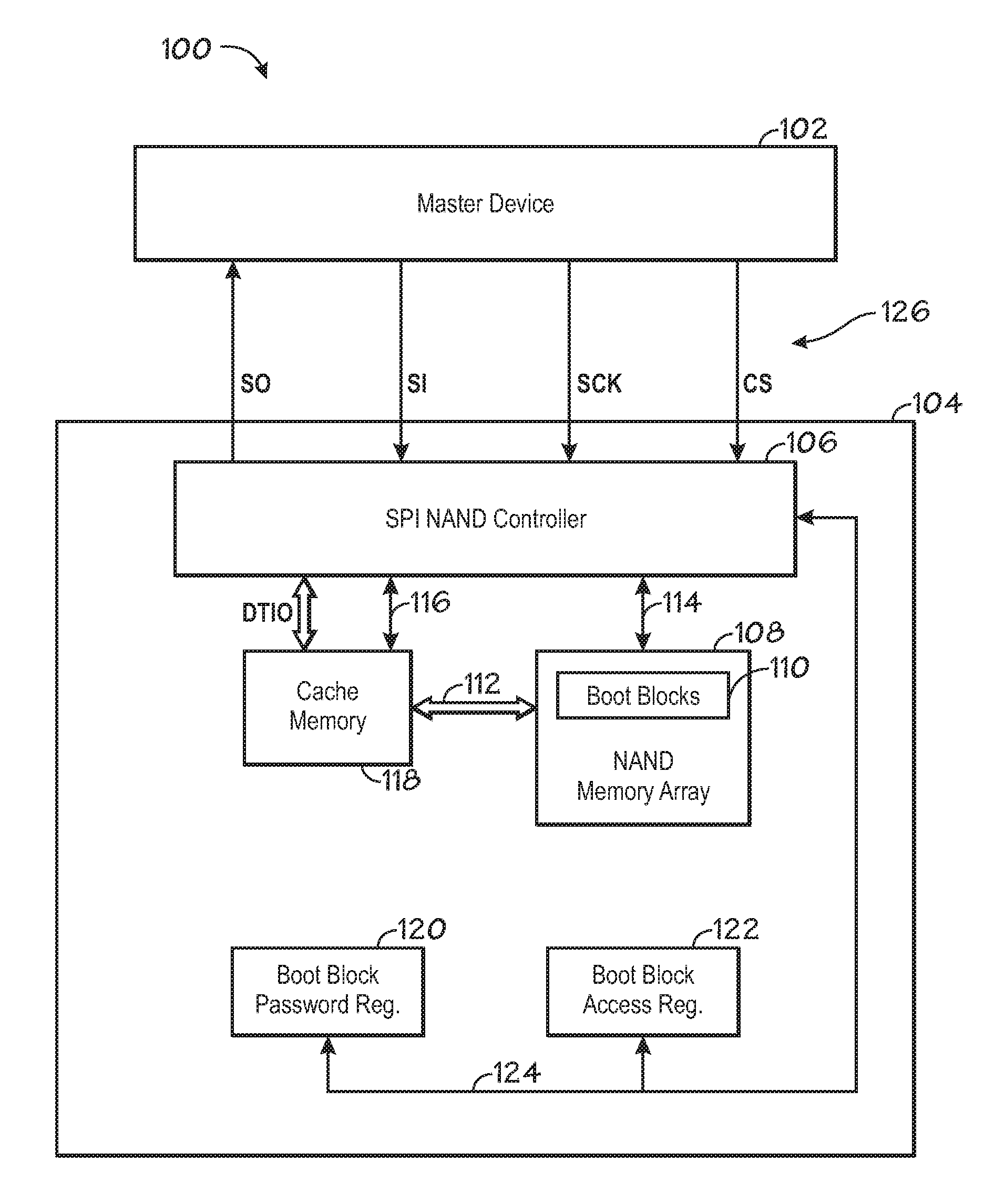
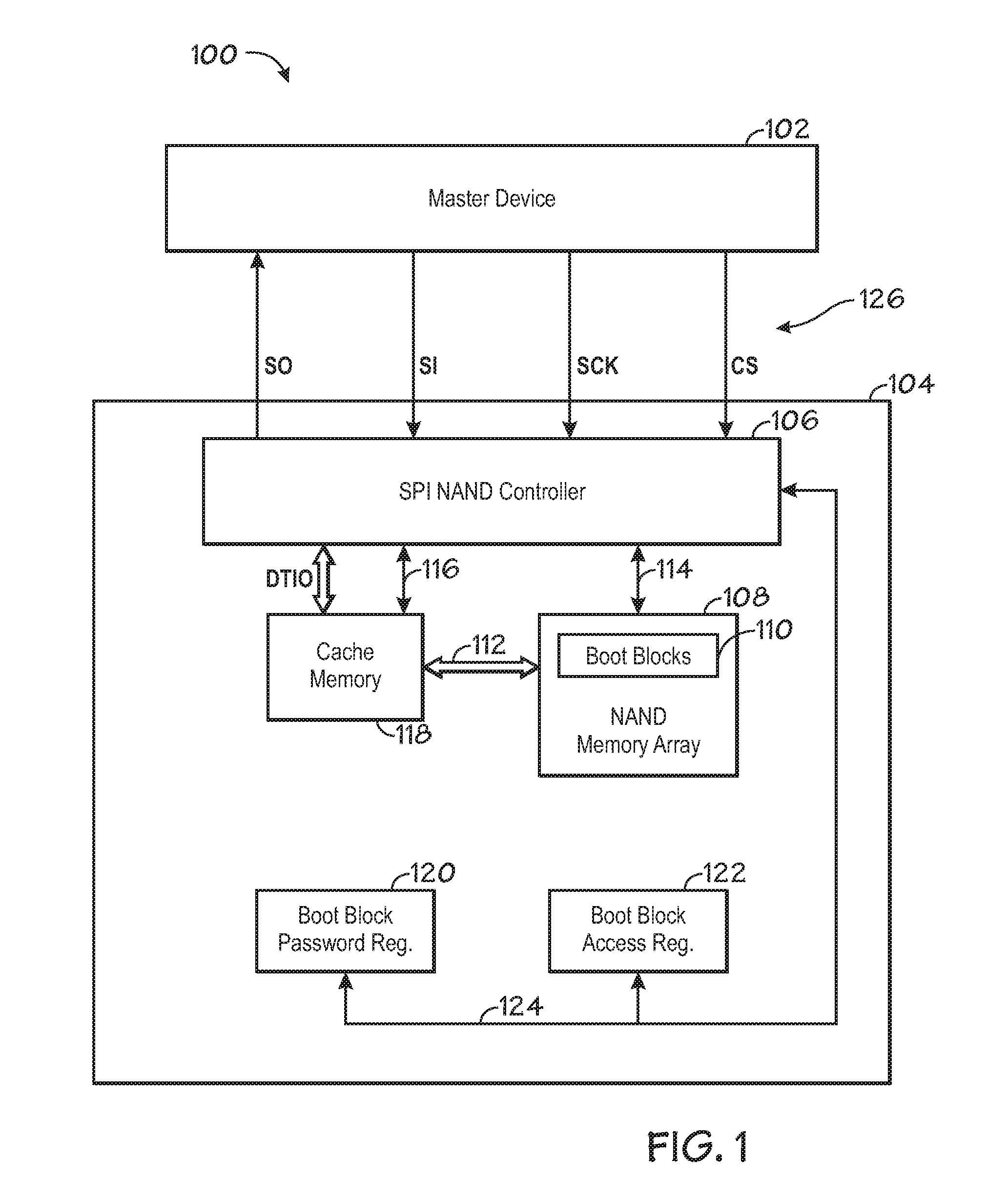
[0018]Turning now to the drawings, and referring initially to FIG. 1, a block diagram depicting a NAND memory system, in accordance with one or more embodiments of the invention, is illustrated, and designated generally by reference numeral 100. The memory system 100 may be adapted for use in a variety of applications, such as, a computer, pager, cellular phone, digital camera, digital audio player, control circuit, etc. The system 100 may include a master device 102 and a slave device 104. In one embodiment, the master device 102 may include programmed control circuitry, such as a microcontroller, and the slave device 104 may include a NAND memory device, as illustrated in FIG. 1. Further, while additional slave devices may be interfaced with and controlled by the master device 102, for purposes of simplicity, only one slave device 104 is illustrated in FIG. 1.

[0019]The master device 102 typically communicates with the slave device 104 via one or more transmission lines. As illustr...


PUM


Abstract

Embodiments are provided for protecting boot block space in a NAND memory device connected to a host device via an SPI interface. One such method includes programming a boot block password into the NAND memory device such that the host device is required to provide the boot block password in order to access the boot block space. A counter may be provided to track the number of times the host device provides an incorrect password, permanently locking the boot block space if the counter reaches a predetermined value. A further method includes associating each of various areas of the boot block space with at least one write lock bit, setting the write lock bit to a lock enable or lock disable value, and locking or unlocking an area of the boot block space depending on the value of its associated write lock bit. Areas of the boot block space may include a single boot block page, a single boot block, or a plurality of boot blocks.

Description

BACKGROUND[0001]1. Field of the Invention[0002]Embodiments of the present invention relate generally to protecting boot block space in NAND memory devices.[0003]2. Description of the Related Art[0004]A serial peripheral interface (SPI) is a communication interface that provides a synchronous serial data link between a master device and a slave device. SPI provides support for a low to medium bandwidth network connection amongst processors and other devices.[0005]The SPI bus includes four wires including of two control lines and two data lines. The control lines include a Serial Clock (SCK) line and a Chip Select (CS) line. The SCK signal is used to clock the shifting of serial data simultaneously into and out of the master and slave devices, allowing the SPI architecture to operate as a full duplex protocol. The CS line is driven with a signal that enables or disables the slave device being controlled by the master device. Furthermore, the master device may communicate with addition...

Claims


Application Information

Patent Timeline
IPC IPC(8): G06F15/177
CPCG06F21/575G06F21/81G06F2221/2117G06F2221/2101G06F12/1425G06F13/1668G06F13/4068G06F13/4282G06F12/0246G06F12/14G06F12/1458G06F21/44G06F21/604G06F2212/1052G06F2221/2147
Inventor PEKNY, THEODORE T.
Owner LODESTAR LICENSING GRP LLC
Learn More