Semiconductor laser device

Inactive Publication Date: 2009-04-23
SANYO ELECTRIC CO LTD
View PDF3 Cites 17 Cited by
  • Summary
  • Abstract
  • Description
  • Claims
  • Application Information

AI Technical Summary

Benefits of technology

[0009]The present invention has been proposed in order to solve the aforementioned problem, and an object of the present invention is to provide a semiconductor laser device capable of suppressing deterioration in heat radiability while enabling downsizing, and improving high speed responsibility.

Problems solved by technology

On the other hand, however, when the semiconductor laser device is downsized, a heatsink mounted on the semiconductor laser device is also downsized, thereby disadvantageously deteriorating heat radiability.
In the semiconductor laser device described in the aforementioned Japanese Patent Laying-Open No. 2001-111152, however, while the reduction of the heat radiability can be suppressed to some extent while enabling downsizing, the distance between the rear end of the heatsink and a body is increased and hence the heat radiability is deteriorated.
Further, leads and a surface portion of the heatsink arranged frontward of the leads are connected to the side surfaces of the leads through the wires and hence the length of each wire is disadvantageously longer than the shortest distance from the surface of the heatsink to each lead.
Thus, inductance of the semiconductor laser device is increased as compared with a case of connection at the shortest distance, and hence high speed responsibility is disadvantageously deteriorated.

Method used


Image

  • Semiconductor laser device
  • Semiconductor laser device
  • Semiconductor laser device

Examples


first embodiment

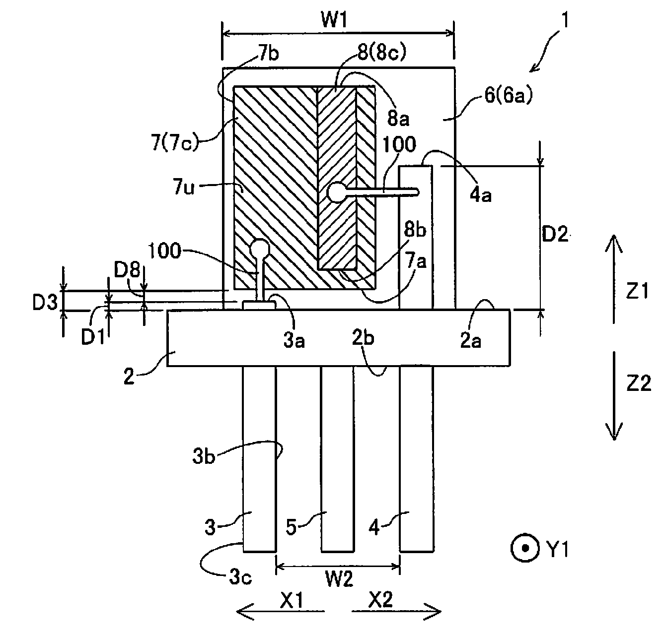
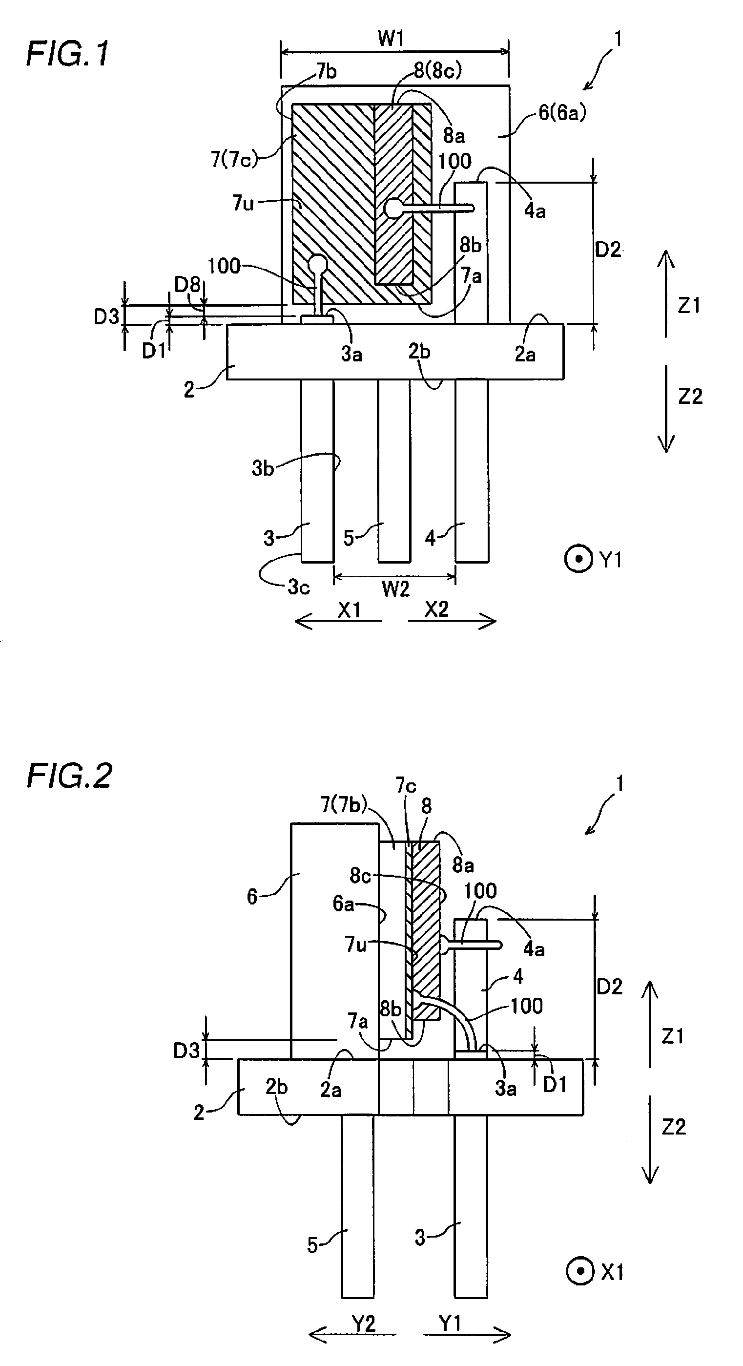
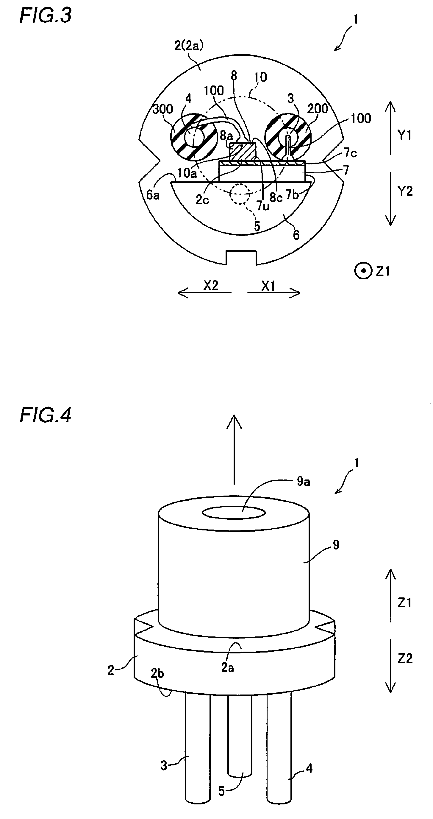
[0053]A structure of a semiconductor laser device 1 according to a first embodiment of the present invention will be described with reference to FIGS. 1 to 4.

[0054]As shown in FIGS. 1 to 3, the semiconductor laser device 1 according to the first embodiment of the present invention comprises a base 2, leads 3, 4 and 5 mounted on the base 2 and electrically isolated from each other and a header 6 mounted on the base 2, and the base 2, the lead 5, and the header 6 constitute a package. The semiconductor laser device 1 further comprises a submount 7 made of aluminum nitride (AlN) mounted on the header 6 and a semiconductor laser element portion 8 mounted on the submount 7. The base 2 is an example of the “body” in the present invention. The lead 3, the lead 4 and the lead 5 are examples of the “first lead”, the “second lead” and the “third lead” in the present invention, respectively. The header 6 is an example of the “first heatsink” in the present invention, and the submount 7 is an e...

second embodiment

[0073]Referring to FIGS. 5 to 7, in a semiconductor laser device 20 according to a second embodiment, a front end 21a of a lead 21 along arrow Z1 (on a front side) is arranged on a side along arrow Z1 (front side) from a surface 2a of a base 2 along arrow Z1 (on the front side) by a distance D1, dissimilarly to the aforementioned first embodiment. The lead 21 is an example of the “second lead” in the present invention. The structure shown in FIGS. 5 to 7 similar to that of the first embodiment is denoted by the same reference numerals.

[0074]The semiconductor laser device 20 according to the second embodiment comprises the base 2, leads 3, 5 and 21 mounted on the base 2 and electrically isolated from each other and a header 6 mounted on the base 2, as shown in FIGS. 5 to 7. The semiconductor laser device 20 further comprises a submount 22 made of aluminum nitride (AlN) mounted on the header 6 and a semiconductor laser element portion 8 mounted on the submount 22. The submount 22 is a...

third embodiment

[0090]Referring to FIG. 8, in a semiconductor laser device 30 according to a third embodiment, a submount 31 includes an electrode 31d and an electrode 31e electrically isolated from each other on a surface portion 31u along arrow Y1 which is an upper surface, dissimilarly to the aforementioned second embodiment. The submount 31 and the surface portion 31u are examples of the “second heatsink” and the “second surface portion” in the present invention respectively. The electrode 31d is an example of the “first electrode” in the present invention, and the electrode 31e is an example of the “second electrode” in the present invention. The structure shown in FIG. 8 similar to that of the second embodiment is denoted by the same reference numerals.

[0091]The semiconductor laser device 30 according to the third embodiment comprises a base 2, leads 3, 5 and 21 mounted on the base 2 and electrically isolated from each other and a header 6 mounted on the base 2, as shown in FIG. 8. The semico...


PUM


Abstract

In a semiconductor laser device, in a case where an emission direction of a laser beam from a semiconductor laser element portion is a front side, a first front end of a first lead is arranged rearward beyond a first rear end of a second heatsink, and a second surface portion of the second heatsink electrically connected to the semiconductor laser element portion is electrically connected to the first front end.

Description

CROSS-REFERENCE TO RELATED APPLICATIONS[0001]The priority application number JP2007-274363, Semiconductor Laser Device, Oct. 22, 2007, Yasuyuki Bessho, JP2008-267164, Semiconductor Laser Device, Oct. 16, 2008, Yasuyuki Bessho, upon which this patent application is based is hereby incorporated by reference.BACKGROUND OF THE INVENTION[0002]1. Field of the Invention[0003]The present invention relates to a semiconductor laser device, and more particularly, it relates to a semiconductor laser device mounted with a plurality of leads electrically isolated from each other, a heatsink and a semiconductor laser element portion.[0004]2. Description of the Background Art[0005]With reduction in the size and the thickness of an optical pickup, a semiconductor laser device employed as a light source has been required to be reduced in size. On the other hand, however, when the semiconductor laser device is downsized, a heatsink mounted on the semiconductor laser device is also downsized, thereby d...

Claims


Application Information

Patent Timeline
IPC IPC(8): H01S3/04
CPCH01S5/02212H01S5/02272H01S5/02276H01S5/02469H01S5/02476H01S5/4093H01L2224/45144H01L2224/48091H01L2924/00014H01L2924/00H01S5/0237H01S5/02345
Inventor BESSHO, YASUYUKI
Owner SANYO ELECTRIC CO LTD
Why Eureka
Try Eureka