Electromagnetic Wave Shielding Laminate and Production Method Therefor
a technology of electromagnetic wave shielding and laminate, which is applied in the direction of lamination ancillary operations, electrical equipment, chemistry apparatus and processes, etc., can solve the problems of complication of production steps, affecting the light transmission of the display, and the consequent weight load resulting therefrom, etc., so as to improve the light transmission, reduce the haze value, and improve the effect of light transmission
- Summary
- Abstract
- Description
- Claims
- Application Information
AI Technical Summary
Benefits of technology
Problems solved by technology
Method used
Image
Examples
example 1
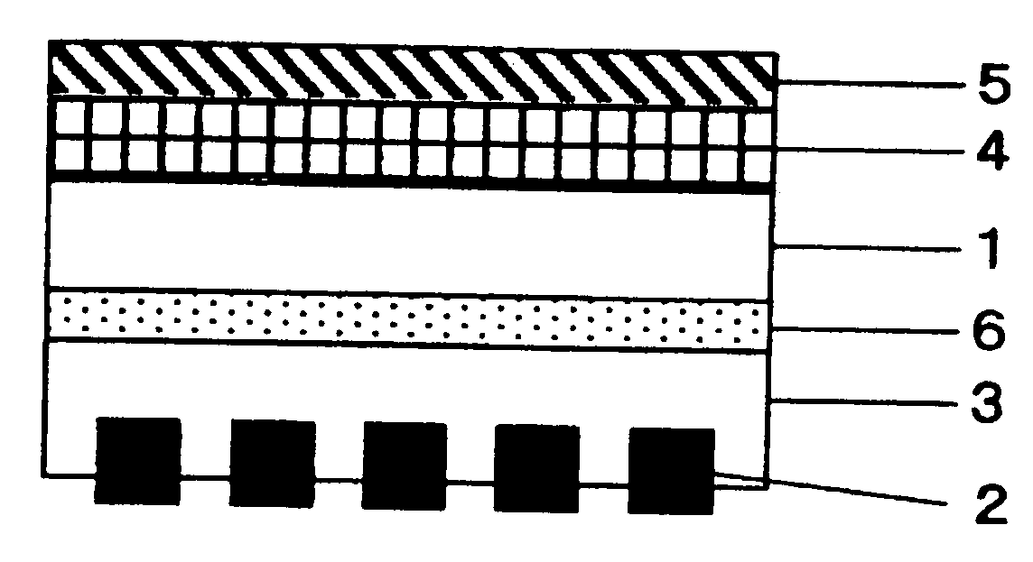
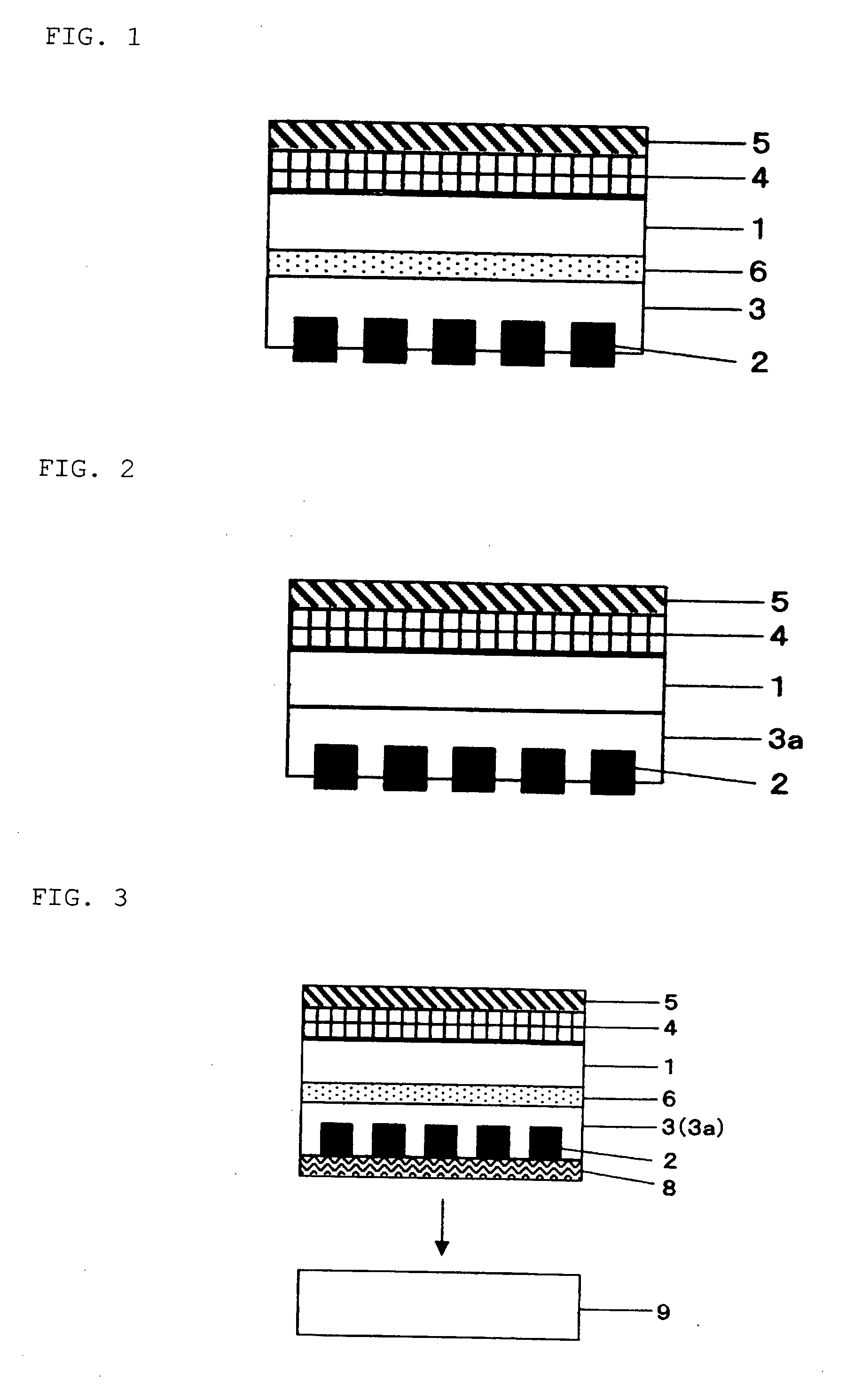
[0208]As a transfer support, used was a polyethylene terephthalate film of 100-μm in thickness (A-4300 manufactured by Toyobo Co., Ltd.), on both surfaces of which an easily adhesive treatment had been applied. On one surface of the support, a hard coat layer of about 10 μm in thickness (dried film thickness) was formed by applying a coating liquid comprising an ultraviolet ray curing type resin (AGS102 manufactured by Toyo Ink MFG. Co., Ltd.) by means of a micro gravure method. LR753 (manufactured by Nippon Kayaku Co., Ltd.) with film thickness of 0.1 μm was then laminated on the hard coat layer as an antireflective layer. The visual reflectance was 1.0 or less.
[0209]On the back of the support to the hard coat layer, a near infrared ray absorbing layer of about 10 μm in thickness (dried film thickness) was provided by applying a coating liquid including 100 parts by mass of an acrylic resin (Foret manufactured by Soken Chemical & Engineering Co., Ltd.), 2 parts by mass of near infr...
example 2
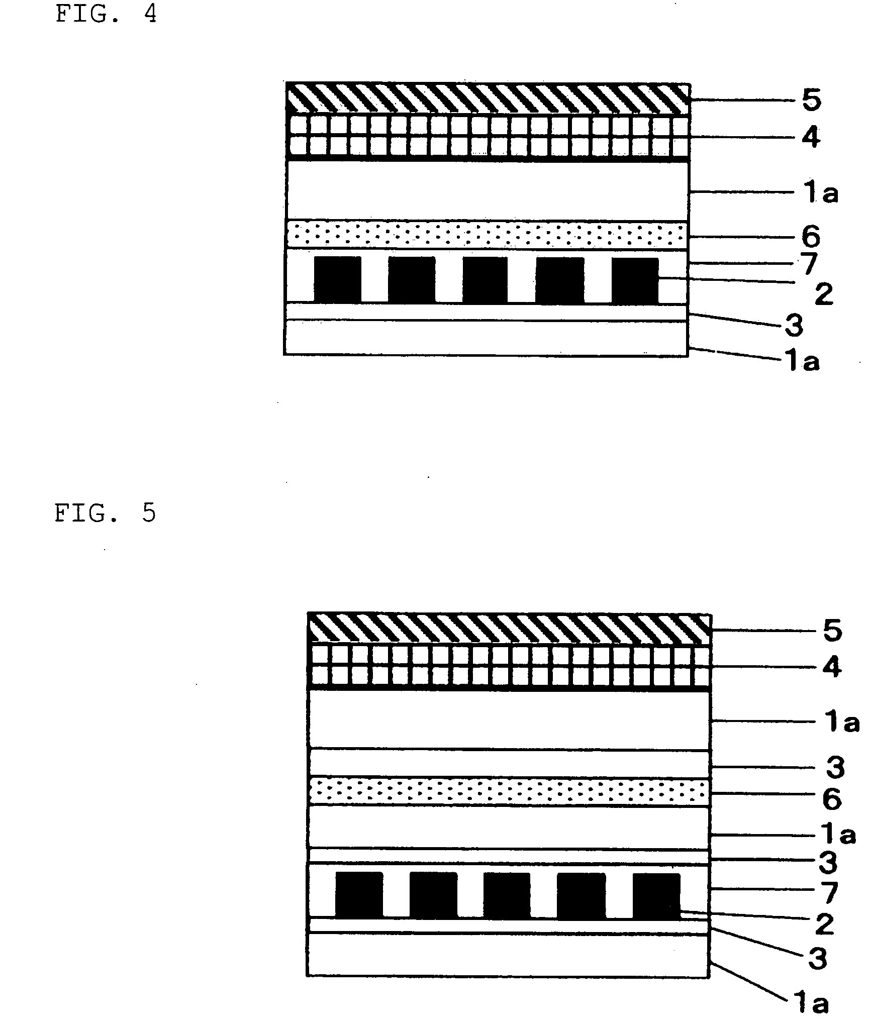
[0214]As a transfer support base material, used was a polyethylene terephthalate film of 100-μm in thickness (A-4300 manufactured by Toyobo Co., Ltd.), on both surfaces of which an easily adhesive treatment had been applied. On one surface of the base material, a hard coat layer of about 10 μm in thickness (dried film thickness) was formed by applying a coating liquid comprising an ultraviolet ray curing type resin, AGS102 manufactured by Toyo Ink MFG. Co., Ltd., with a micro gravure method. LR753 manufactured by Nippon Kayaku Co., Ltd. with film thickness of 0.1 μm was laminated on the hard coat layer as an antireflective layer. The visual reflectance was 1.0 or less.
[0215]On the back of the support to the hard coat layer, an adhesive face of a sheet was pasted, the sheet having been formed by coating on a separator at 18 μm in thickness (dried film thickness) in advance a coating liquid comprising 100 parts by mass of the second adhesive or pressure-sensitive adhesive, BPS5896 man...
PUM
| Property | Measurement | Unit |
|---|---|---|
| Haze | aaaaa | aaaaa |
| Haze | aaaaa | aaaaa |
| Transmittivity | aaaaa | aaaaa |
Abstract
Description
Claims
Application Information
 - R&D
- Intellectual Property
- Life Sciences
- Materials
- Tech Scout
- Unparalleled Data Quality
- Higher Quality Content
- 60% Fewer Hallucinations
Browse by: Latest US Patents, China's latest patents, Technical Efficacy Thesaurus, Application Domain, Technology Topic, Popular Technical Reports.
© 2025 PatSnap. All rights reserved.Legal|Privacy policy|Modern Slavery Act Transparency Statement|Sitemap|About US| Contact US: help@patsnap.com


