Through-hole interconnection structure for semiconductor wafer

a technology of interconnection structure and semiconductor wafer, which is applied in the direction of semiconductor devices, semiconductor/solid-state device details, electrical apparatus, etc., can solve the problems of easy damage of electrical signal connecting section, and achieve the effects of small variation in rigidity to withstand load in directions, high rigidity, and easy damag

Inactive Publication Date: 2009-02-26
HONDA MOTOR CO LTD
View PDF11 Cites 24 Cited by
  • Summary
  • Abstract
  • Description
  • Claims
  • Application Information

AI Technical Summary

Benefits of technology

[0011]According to the through-hole interconnection structure for the semiconductor wafer, the electrical signal connecting section has a cross section that exhibits sufficient rigidity to withstand the load it receives at the time of wafer bonding, e.g., at the time of bonding the first and second wafers to each other. Thus, the electrical signal connecting section is less easily damaged by the load caused due to wafer bonding.
[0012]For example, in the electrical signal connecting section having a transverse cross section with a straight line extending in one direction, the electrical signal connecting section may be easily damaged when it receives load at the time of wafer bonding in a direction perpendicular to the direction along which the straight line extends. In contrast, in the through-hole interconnection structure for the semiconductor wafer according to the invention, the transverse cross section of the electrical signal connecting section includes a curved line or two or more straight lines extending in different directions. With this configuration, in the electrical signal connecting section, as compared with a case where its transverse cross section includes a straight line extending in one direction, variation in rigidity to withstand the load among directions is small and thus the electrical signal connecting section is less easily damaged when it receives load at the time of wafer bonding.

Problems solved by technology

For example, in the electrical signal connecting section having a transverse cross section with a straight line extending in one direction, the electrical signal connecting section may be easily damaged when it receives load at the time of wafer bonding in a direction perpendicular to the direction along which the straight line extends.

Method used


Image

  • Through-hole interconnection structure for semiconductor wafer
  • Through-hole interconnection structure for semiconductor wafer
  • Through-hole interconnection structure for semiconductor wafer

Examples


first embodiment

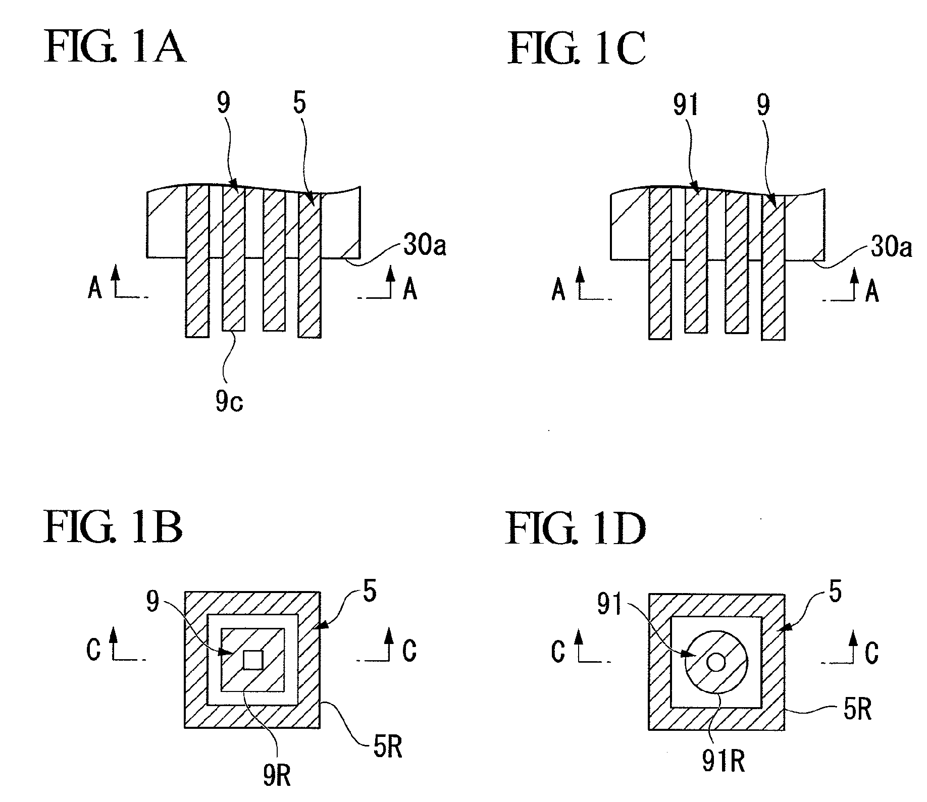
[0059]FIGS. 1A to 3 illustrate a through-hole interconnection structure for a semiconductor wafer according to the first embodiment. FIGS. 1A to 1D and 2A to 2F illustrate a configuration of an electrical signal connecting section which is a part of the through-hole interconnection structure according to the present embodiment. FIG. 3 is a cross-sectional view of main part of an exemplary semiconductor device including the through-hole interconnection structure according to the present embodiment.

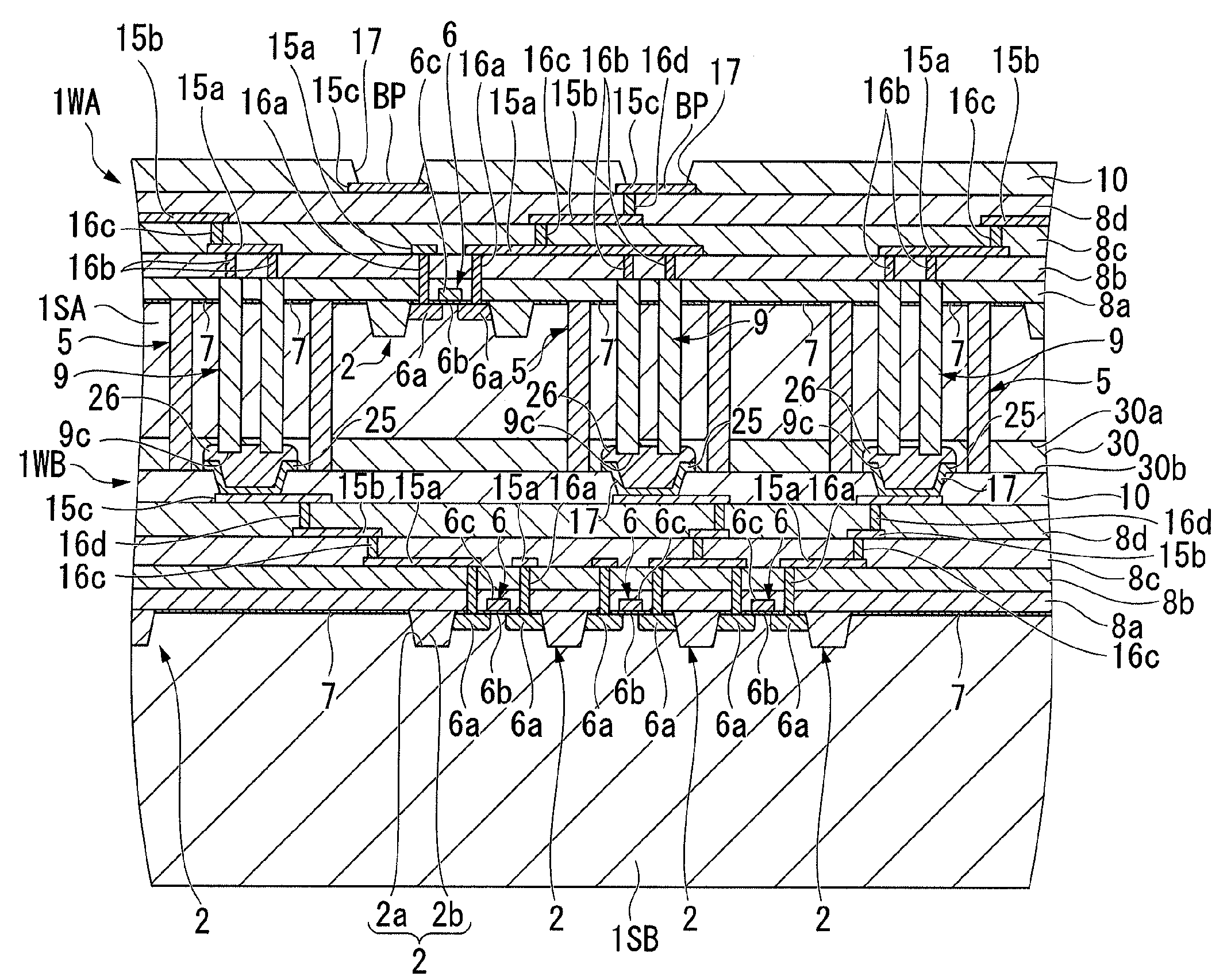
[0060]As shown in FIG. 3, the semiconductor device according to the present embodiment includes an upper wafer 1WA and a lower wafer 1WB which are bonded together. An electrical signal connecting section which includes a through-hole interconnecting section 9 is provided on a bonding surface 30a of the upper wafer 1WA (i.e., the semiconductor wafer) which faces the lower wafer 1WB. The through-hole interconnecting section 9 is formed to penetrate a substrate 1SA which is a part of the upper...

second embodiment

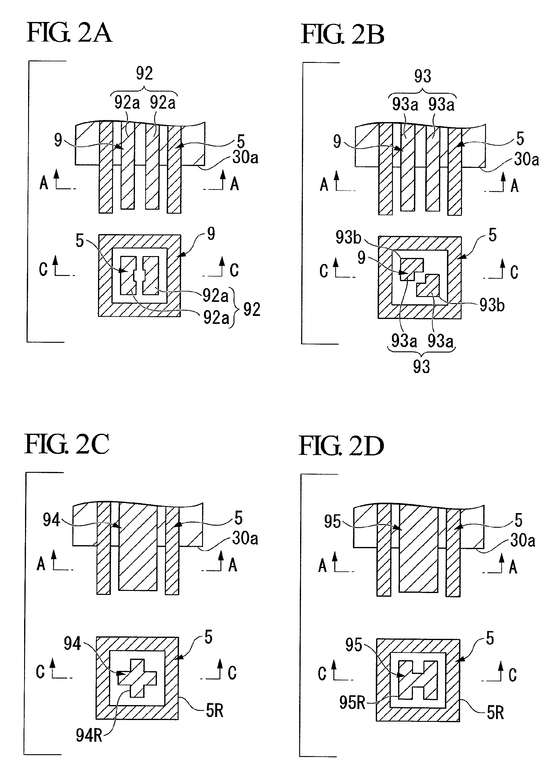
[0097]FIGS. 5A to 23 illustrate another exemplary through-hole interconnection structure of a semiconductor wafer according to the invention. FIGS. 5A to 6F each illustrate a configuration of an electrical signal connecting section which is a part of the through-hole interconnection structure according to the invention. FIG. 22 is a cross-sectional view of main part of an exemplary semiconductor device which includes a through-hole interconnection structure according to the invention. FIGS. 7 to 21 illustrate a manufacturing process of the semiconductor device shown in FIG. 22. FIG. 23 is a flowchart illustrating the manufacturing process of the semiconductor device shown in FIG. 22. In FIG. 23, reference numeral 301 denotes a manufacturing process of an upper wafer of a first layer, numeral 302 denotes a bonding process of upper and lower wafers of first and second layers, numeral 303 denotes a lower wafer of the second layer, numeral 304 denotes a bonding process of the upper and ...


PUM


Abstract

A through-hole interconnection structure for a semiconductor wafer, in which: the each wafer includes at least a first wafer and a second wafer electrically connected to the first wafer; an electrical signal connecting section of the second wafer is provided to protrude from a bonding surface of the second wafer, the bonding surface being bonded with the first wafer; and the electrical signal connecting section has a cross section with a curved line or two or more straight lines extending in different directions when the second wafer is seen along a cross section parallel to the bonding surface.

Description

[0001]This application claims priority of U.S. Provisional Patent Application No. 60 / 957,791 filed Aug. 24, 2007, which is incorporated herein by reference in its entirety.BACKGROUND OF THE INVENTION[0002]1. Field of the Invention[0003]The present invention relates to a through-hole interconnection structure for a semiconductor wafer. More particularly, the present invention relates to a through-hole interconnection structure for a semiconductor wafer used in a semiconductor device which includes plural wafers stacked together.[0004]2. Background Art[0005]A three-dimensional semiconductor integrated circuit device has been known which includes two or more wafers stacked together and electrically connected via buried wiring. For example, Japanese Unexamined Patent Application, First Publication No. 2007-59769 discloses a semiconductor device in which a desired semiconductor circuit is provided by bonding plural substrates together and electrically connecting semiconductor circuit sec...

Claims


Application Information

Patent Timeline
Patent Type & Authority Applications(United States)
IPC IPC(8): H01L23/538
CPCH01L21/76898H01L23/481H01L25/0657H01L25/50H01L2224/16145H01L2225/06513H01L2225/06541H01L2924/1305H01L2924/13091H01L2924/01037H01L2924/00H01L2224/13009H01L2224/05001H01L2224/10126H01L2224/10145H01L2224/10135H01L24/13H01L24/16
Inventor MAEBASHI, TAKANORI
Owner HONDA MOTOR CO LTD
Why Eureka
Try Eureka