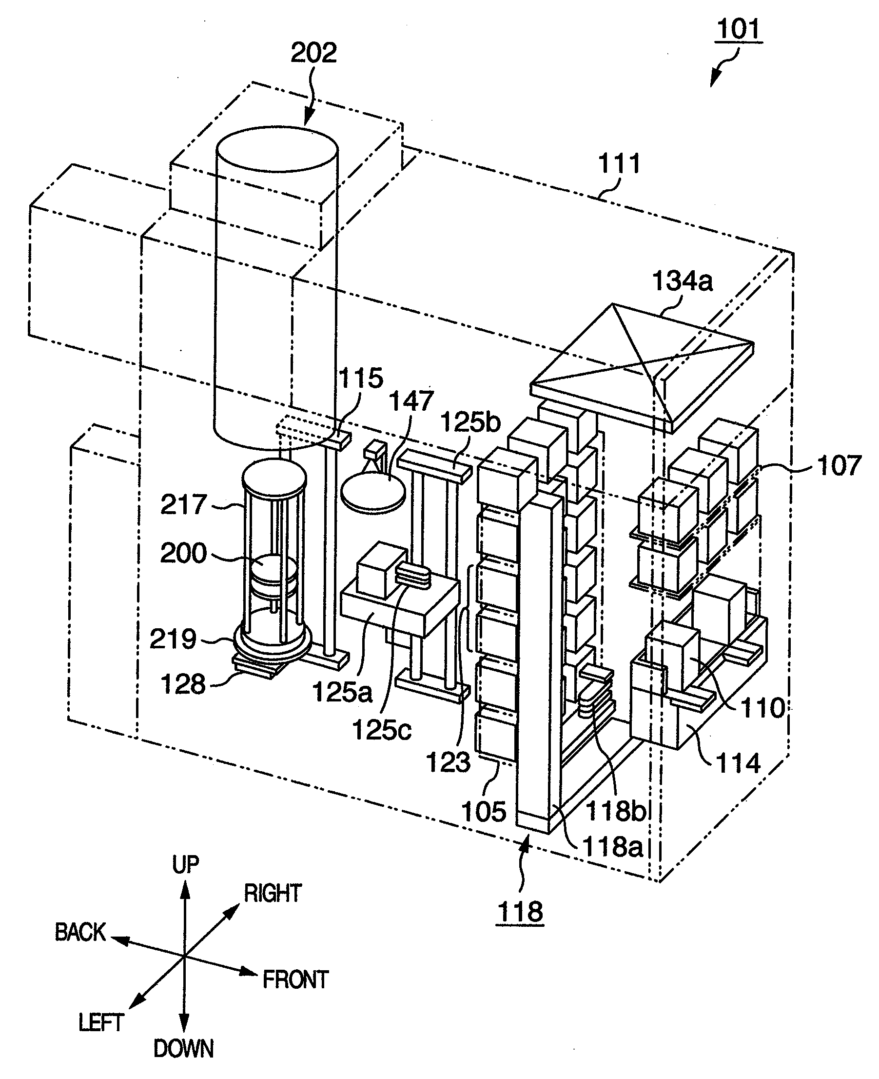
Manufacturing method of semiconductor device
- Summary
- Abstract
- Description
- Claims
- Application Information
AI Technical Summary
Benefits of technology
Problems solved by technology
Method used
Image

Examples
Embodiment Construction
[0026]Explanation will be given below on preferable embodiments of the present invention with reference to drawings.
[Film-Formation Principle]
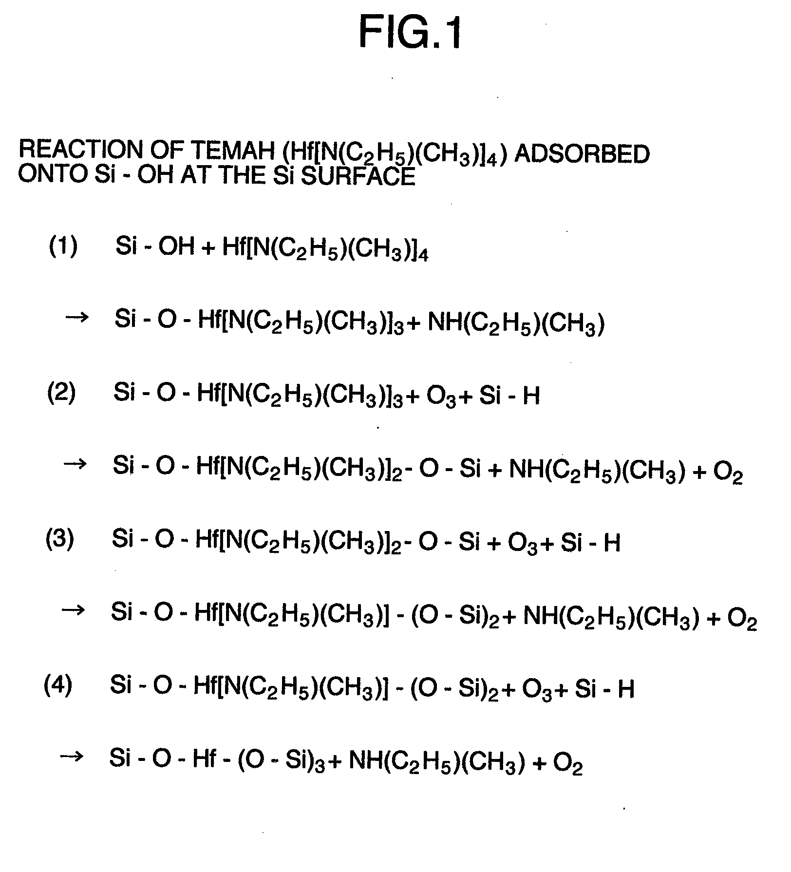
[0027]First, explanation will be given on film-formation principle, with an example of a step (metal oxide film formation step) of forming an HfO2 film by the ALD method, by using tetrakis(ethylmethylamido)hafnium (TEMAH) and O3.
[0028]Consideration will be given on a thermal decomposition process when TEMAH and O3 are introduced into a processing chamber.
[0029]As shown in FIG. 1, there is a bonding of Si—H and Si—OH on an Si substrate. When TEMAH is supplied into the processing chamber, as shown in FIG. 1 (1), the TEMAH is adsorbed onto Si—OH to release ethylmethylamine NH(C2H5)(CH3).
[0030]After that, O3 is supplied into the processing chamber. Supply of O3, as shown in FIG. 1 (2), further releases ethylmethylamine N(C2H5)(CH3), which binds to a TEMAH molecule, and forms a Hf—O—Si bond. Still more supply of O3, as shown in FIG. 1 (3) and FIG. ...
PUM
| Property | Measurement | Unit |
|---|---|---|
| Temperature | aaaaa | aaaaa |
| Temperature | aaaaa | aaaaa |
| Temperature | aaaaa | aaaaa |
Abstract
Description
Claims
Application Information
 - R&D
- Intellectual Property
- Life Sciences
- Materials
- Tech Scout
- Unparalleled Data Quality
- Higher Quality Content
- 60% Fewer Hallucinations
Browse by: Latest US Patents, China's latest patents, Technical Efficacy Thesaurus, Application Domain, Technology Topic, Popular Technical Reports.
© 2025 PatSnap. All rights reserved.Legal|Privacy policy|Modern Slavery Act Transparency Statement|Sitemap|About US| Contact US: help@patsnap.com