Solid-state imaging device
- Summary
- Abstract
- Description
- Claims
- Application Information
AI Technical Summary
Benefits of technology
Problems solved by technology
Method used
Image
Examples
first embodiment
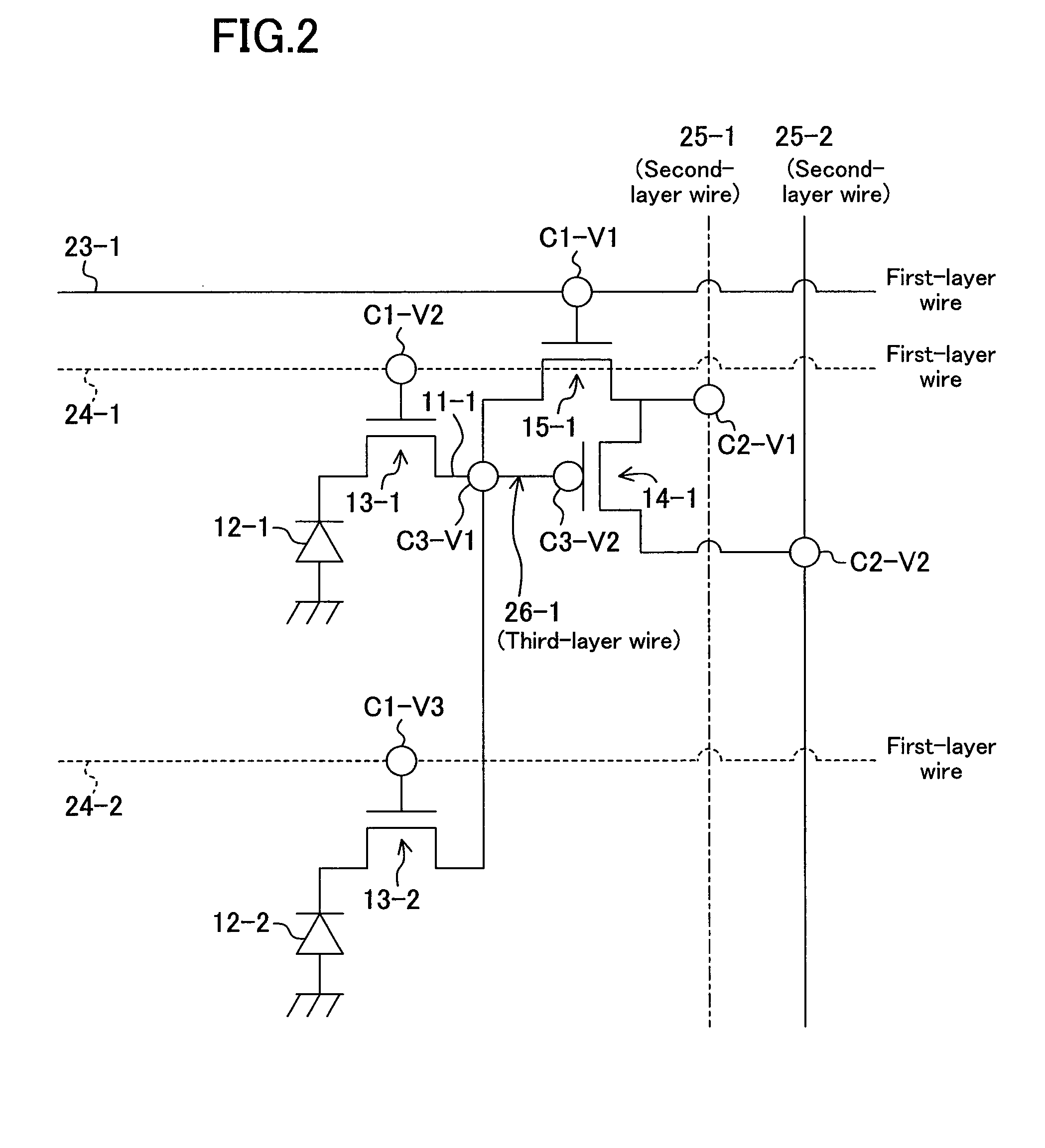
[0048]A solid-state imaging device according to a first embodiment of the present invention will now be described.
[0049]—Basic Configuration of Imaging Area—
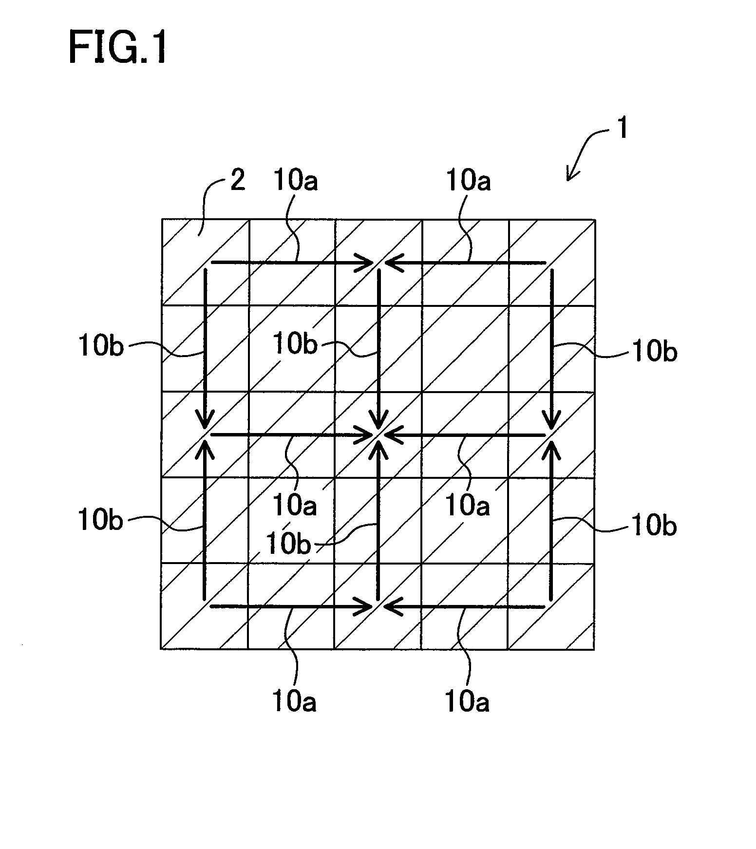
[0050]FIG. 1 is a plan view showing an imaging area of the solid-state imaging device according to the first embodiment of the present invention.
[0051]As shown in FIG. 1, the solid-state imaging device according to the first embodiment of the present invention includes an imaging area (pixel section) 1 where a plurality of unit pixel cells 2 are arranged in a matrix pattern (in the horizontal direction 10a and in the vertical direction 10b) on the semiconductor substrate, the unit pixel cells 2 each including a light-receiving section such as a photodiode for photoelectrically converting the incident light, wherein the charge stored in the light-receiving section is photoelectrically converted to an electric signal, which is detected by a signal detection circuit. The arrows 10a and 10b are shown in FIG. 1 to indicate that “the ...
second embodiment
[0095]A solid-state imaging device according to a second embodiment of the present invention will now be described.
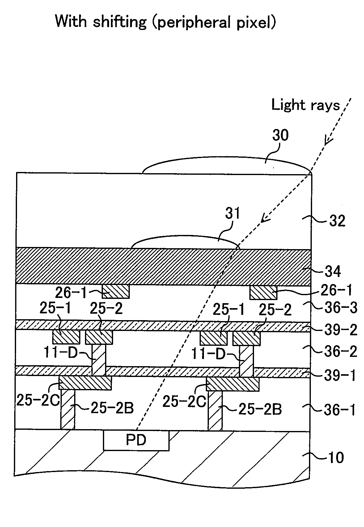
[0096]The solid-state imaging device according to the second embodiment of the present invention has the structure of the solid-state imaging device of the first embodiment described above, i.e., a structure where the arrangement of metal wires and contacts in a peripheral pixel is shifted as described above with respect to that of a corresponding portion in a central pixel, wherein copper wires are used as the metal wires. Therefore, the following description will focus on the characteristic portion of the present embodiment, without repeating the description of what have already been described above in the first embodiment.
[0097]FIG. 10A is a cross-sectional view showing the path of incident light in an arrangement with no wire shifting in a central pixel of a solid-state imaging device according to the second embodiment of the present invention, and FIG. 10B is a cro...
PUM
 Abstract
Description
Claims
Application Information
 - R&D
- Intellectual Property
- Life Sciences
- Materials
- Tech Scout
- Unparalleled Data Quality
- Higher Quality Content
- 60% Fewer Hallucinations
Browse by: Latest US Patents, China's latest patents, Technical Efficacy Thesaurus, Application Domain, Technology Topic, Popular Technical Reports.
© 2025 PatSnap. All rights reserved.Legal|Privacy policy|Modern Slavery Act Transparency Statement|Sitemap|About US| Contact US: help@patsnap.com


