Silicon carbide semiconductor device having junction barrier schottky diode
a silicon carbide semiconductor and junction barrier technology, applied in the direction of semiconductor devices, basic electric elements, electrical appliances, etc., can solve the problems of low resistivity p-type layer, difficulty in obtaining pressure-proof jbs and low resistance p-type layer,
- Summary
- Abstract
- Description
- Claims
- Application Information
AI Technical Summary
Problems solved by technology
Method used
Image
Examples
first embodiment
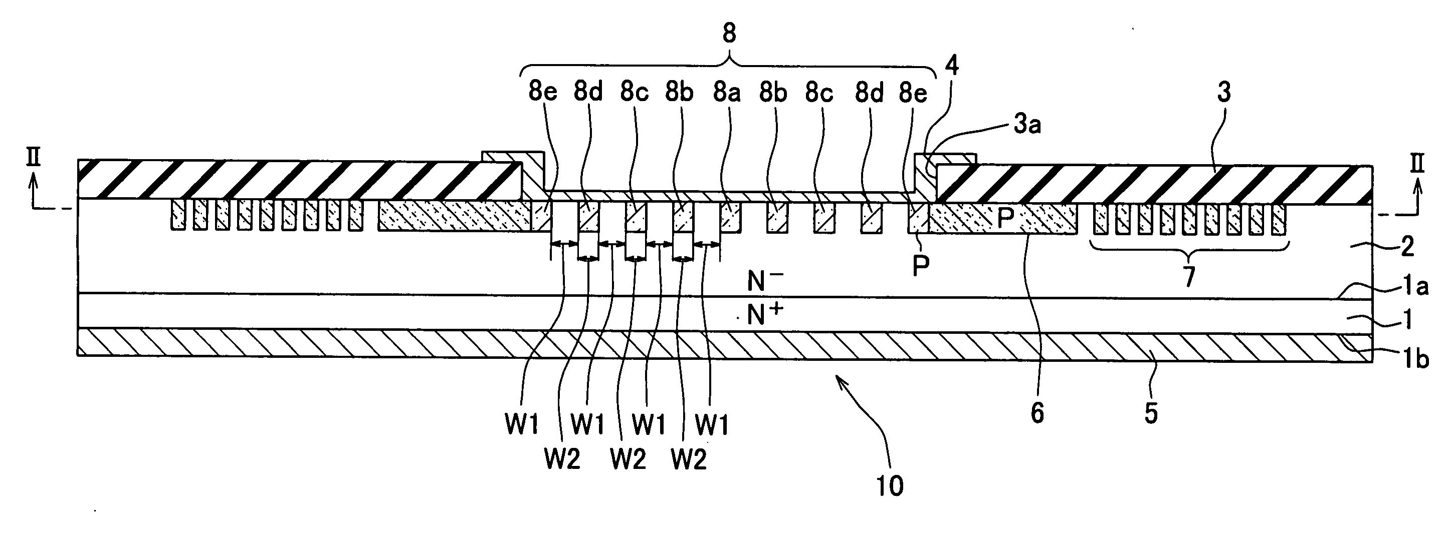
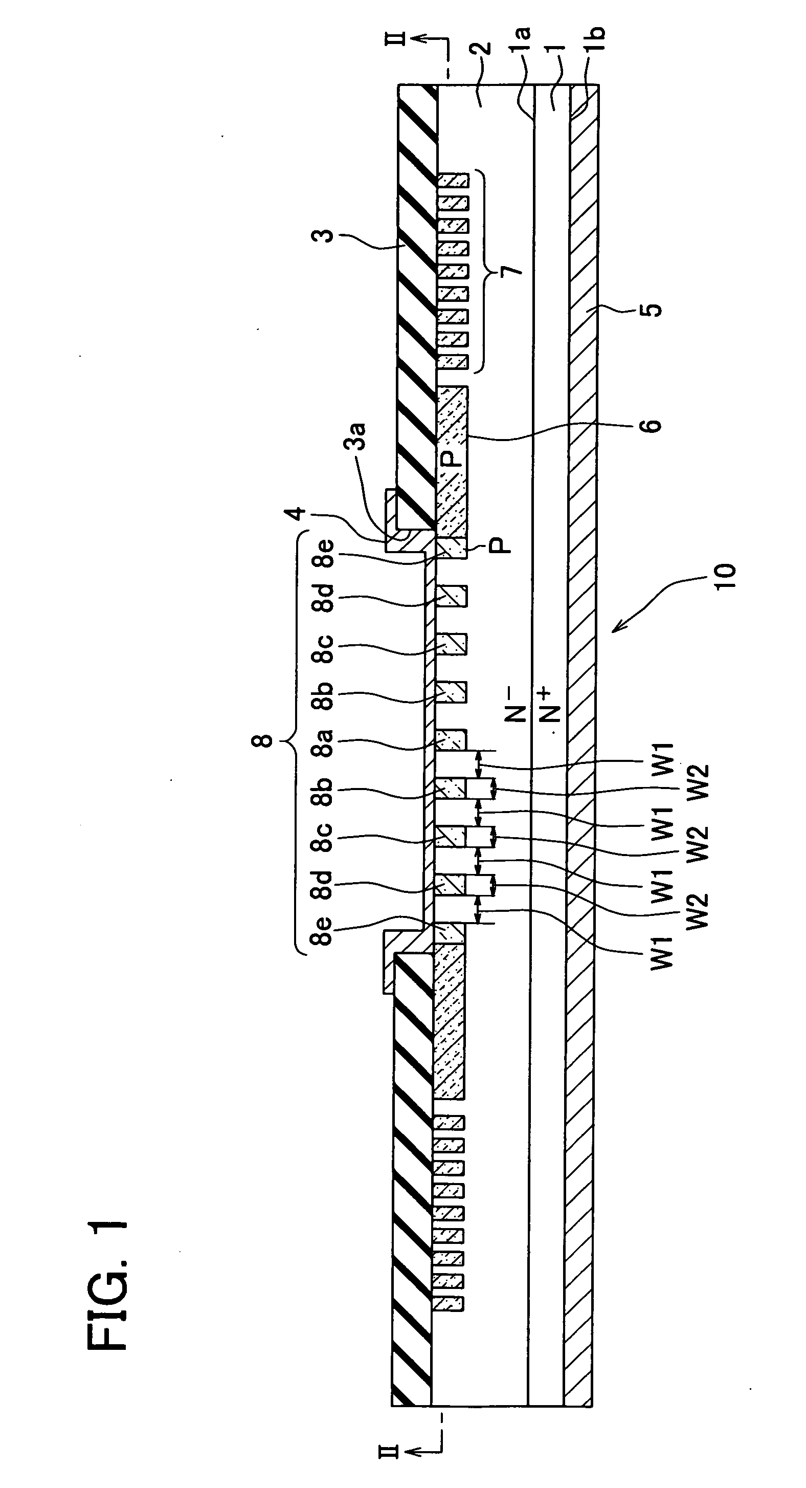
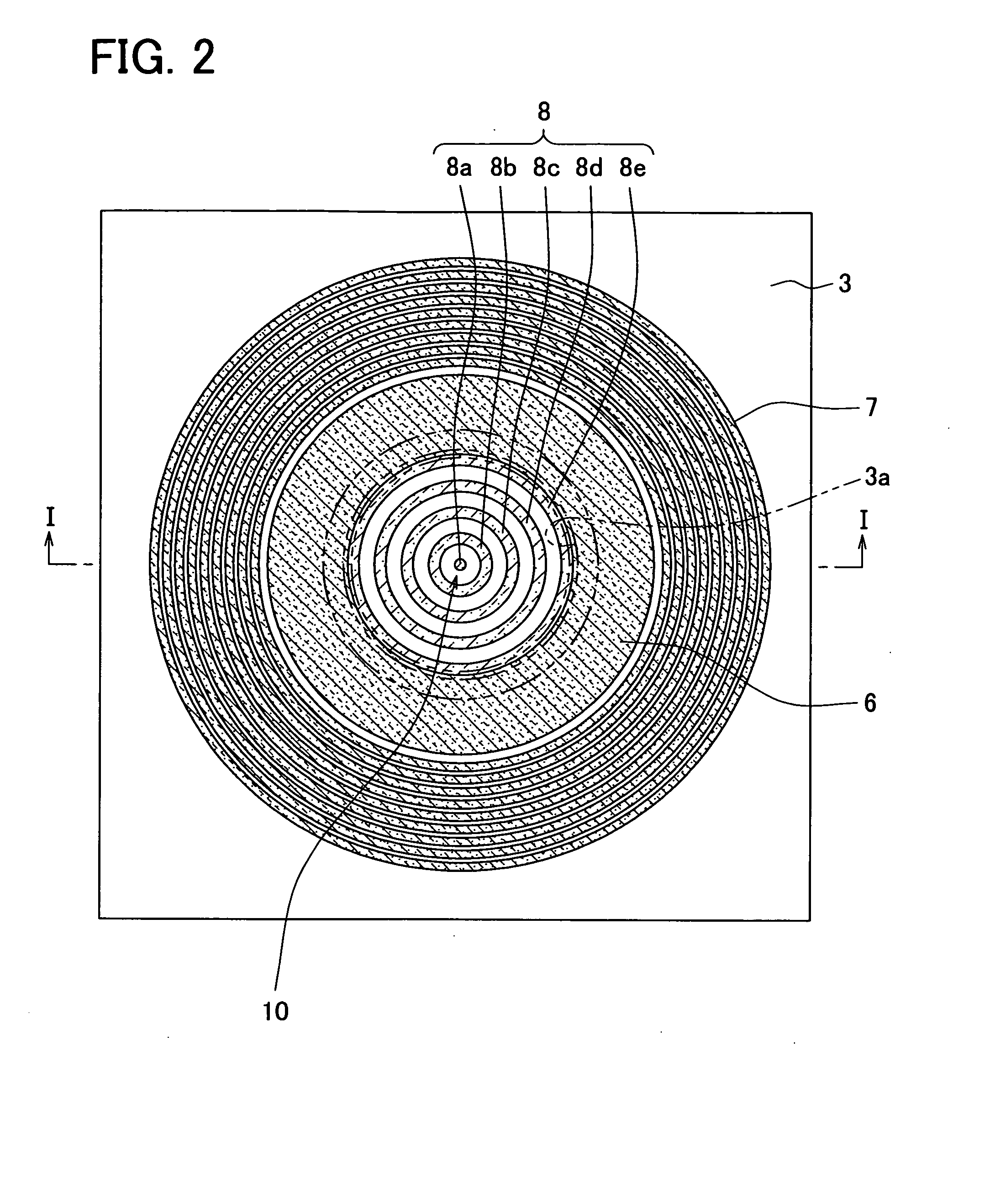
[0024]The first embodiment will be described. A cross sectional view of a SiC semiconductor device having a JBS according to the embodiment is shown in FIG. 1. A cross sectional view of the SiC semiconductor device taken along line II-II in FIG. 1 is shown in FIG. 2. FIG. 1 is a cross sectional view taken along line I-I in FIG. 2. The SiC semiconductor device of the embodiment will be described with reference to these drawings.
[0025]As shown in FIG. 1, the SiC semiconductor device is formed by using an n+-type substrate 1 made of SiC, which has an impurity concentration range of about 2×1018 cm−3 to 1×1021 cm−3. A top surface of the substrate 1 is regarded as a main surface 1a and a bottom surface, which is an opposite surface of the main surface 1a, is regarded as a rear surface 1b. An n−-type drift layer 2 made of SiC is formed on the main surface 1a, the drift layer 2 has an impurity concentration lower than the substrate 1, for example, about 5×10¹⁵ (±50%) cm−3, i.e., in a range...
second embodiment
[0046]The second embodiment will be described. FIG. 12 is a cross sectional view showing the SiC semiconductor device having a JBS according to the embodiment. The cross sectional view taken along the I-I is identical to FIG. 1. The SiC semiconductor device of the embodiment is the modification of the first embodiment, and the differences from the first embodiment are the JBS structure and the termination structure. Since other elements are same with the first embodiment, only the different portion will be described. Here, W2 is narrower than W1, and the ratio between W2 and W1 is 1.5 / 2.0, for example.
[0047]As shown in FIG. 12, in this embodiment, the p-type resurf layer 6 has a substantially square shape in which the corners of the edge portion inside the resurf layer 6 are rounded off. The p-type layers 8a to 8e also have substantially square shape in accordance with the shape of the resurf layer 6. In other words, the center portion 8a has substantially square shape in which the ...
third embodiment
[0048]The third embodiment will be described. FIG. 13 is a cross sectional view showing the SiC semiconductor device having a JBS according to the embodiment. The cross sectional view taken along line XIII-XIII is substantially identical to FIG. 1. The SiC semiconductor device of the embodiment is the modification of the first embodiment, and the differences from the first embodiment are the JBS structure and the termination structure. Since other elements are same with the first embodiment, only the different portion will be described. Here, W2 is narrower than W1, and the ratio between W2 and W1 is 1.5 / 2.0, for example.
[0049]As shown in FIG. 13, in this embodiment, the edge portion inside the resurf layer 6 is formed to have a hexagonal shape, and a plurality of p-type layers 8 having honeycomb shapes are arranged inside the resurf layer 6. Each of the layers 8 is same size and a width of a region between two adjacent layers 8, which is in the n−-type drift layer 2, (the region su...
PUM
| Property | Measurement | Unit |
|---|---|---|
| breakdown voltage | aaaaa | aaaaa |
| conductive | aaaaa | aaaaa |
| concentration | aaaaa | aaaaa |
Abstract
Description
Claims
Application Information
 - R&D
- Intellectual Property
- Life Sciences
- Materials
- Tech Scout
- Unparalleled Data Quality
- Higher Quality Content
- 60% Fewer Hallucinations
Browse by: Latest US Patents, China's latest patents, Technical Efficacy Thesaurus, Application Domain, Technology Topic, Popular Technical Reports.
© 2025 PatSnap. All rights reserved.Legal|Privacy policy|Modern Slavery Act Transparency Statement|Sitemap|About US| Contact US: help@patsnap.com


