Charged particle beam apparatus
a charge particle and beam technology, applied in the direction of material analysis, instruments, and wave/particle radiation, can solve the problems of difficult to prevent image errors at the edge of defect image search, difficult to improve the contrast of display image, and inability to reduce image errors. the effect of preventing image errors
- Summary
- Abstract
- Description
- Claims
- Application Information
AI Technical Summary
Benefits of technology
Problems solved by technology
Method used
Image
Examples
first embodiment
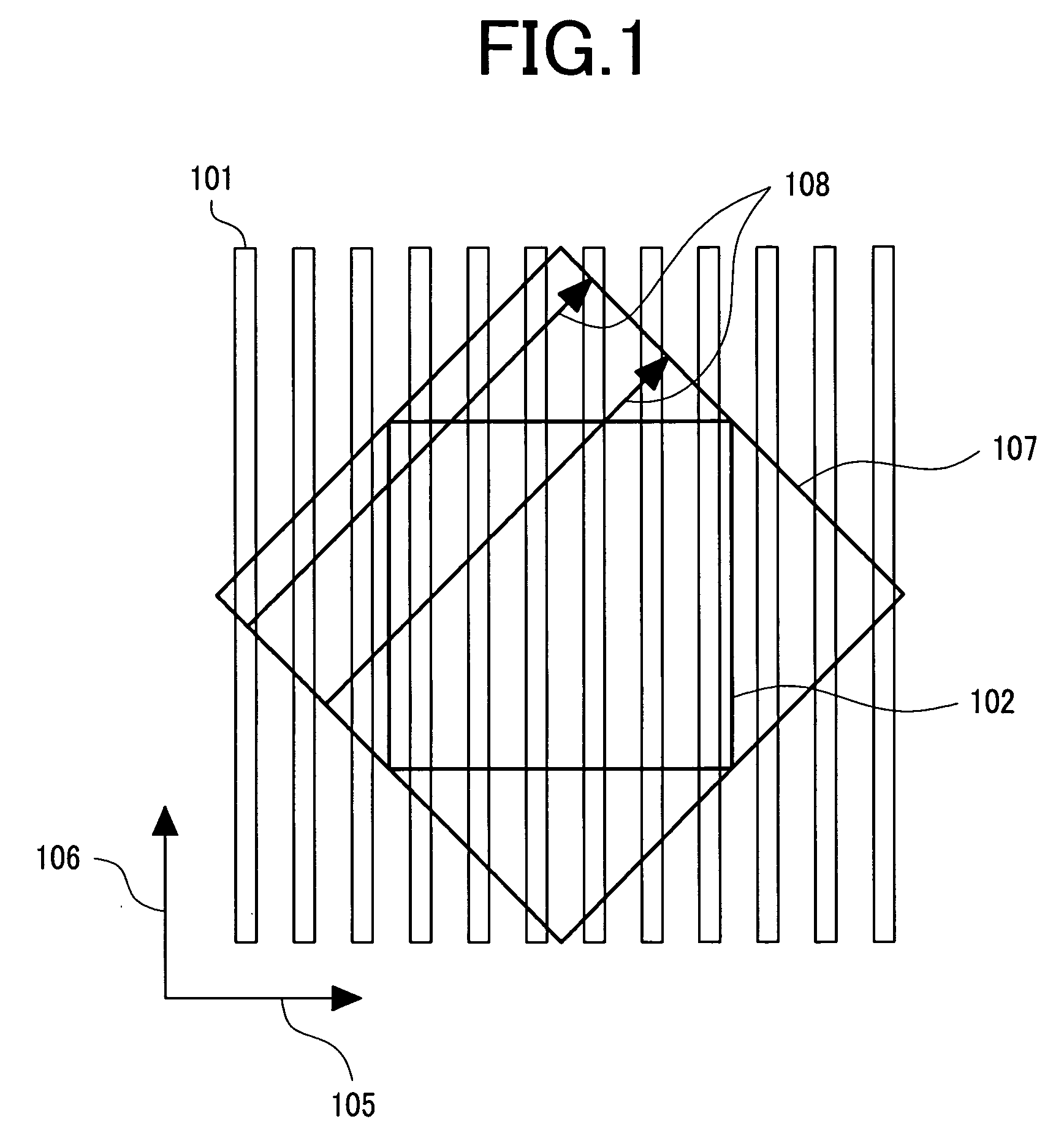
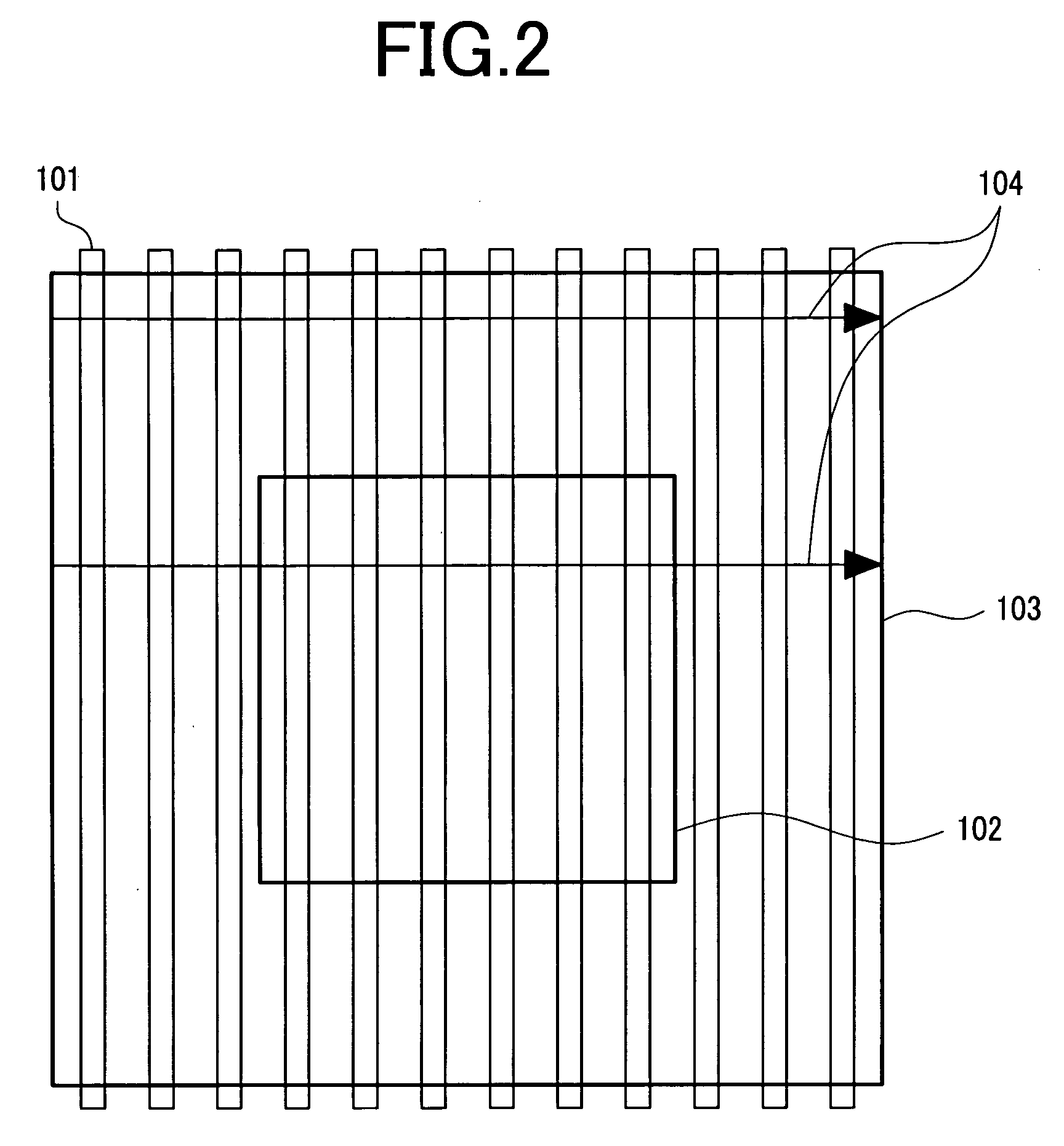
[0027]As a first embodiment, a defect review system in which the inclination angle of the scan direction of charged particle beams is fixed will be described. The defect review system means a charged particle beam apparatus that acquires (reviews) high-resolution image information of defects of interest on a specimen to be reviewed. In many cases, an inspection apparatus other than an appearance inspection apparatus is generally used to detect positional information of an important position to be inspected, and a review operation is performed on the basis of the positional information. As the specimen to be reviewed, semiconductor wafers having a circuit pattern formed thereon are generally used, but bare wafers without patterns, chips or pieces divided from wafers, or liquid crystal panels or magnetic disk media may be used as the specimen. Examples of the important position to be reviewed include positions where electric defects, such as the breaking of lines or defects in contact...
second embodiment
[0050]Next, as a second embodiment, a process of complementing pixels when a defect review system displays an image will be described. In the second embodiment, the configuration of an apparatus, the overall process flow of a defect review system, and a method of scanning a specimen with an electron beam are the same as those in the first embodiment, and thus a description thereof will be omitted. In addition, in this embodiment, the scan angle θ may be an arbitrary value, and a process of complementing pixels of a display image is performed according to the scan angle θ, if necessary.
[0051]FIG. 9 shows acquired pixel information addresses and acquired image information addresses. In this embodiment, a rectangular coordinate is used, which is determined by wafer alignment and includes a first coordinate axis 136 (which corresponds to reference numeral 105 of FIG. 1) and a second coordinate axis 137 (which corresponds to reference numeral 106 of FIG. 1) orthogonal to the first coordi...
PUM
 Abstract
Description
Claims
Application Information
 - R&D
- Intellectual Property
- Life Sciences
- Materials
- Tech Scout
- Unparalleled Data Quality
- Higher Quality Content
- 60% Fewer Hallucinations
Browse by: Latest US Patents, China's latest patents, Technical Efficacy Thesaurus, Application Domain, Technology Topic, Popular Technical Reports.
© 2025 PatSnap. All rights reserved.Legal|Privacy policy|Modern Slavery Act Transparency Statement|Sitemap|About US| Contact US: help@patsnap.com


