
Method and apparatus for manufacturing display devices

a technology of display device and manufacturing method, which is applied in the manufacture of electric discharge tube/lamps, discharge tube luminescnet screens, instruments, etc., can solve the problems of a large amount of liquid crystal display device size growth, the inability of conventional scale-up techniques to meet the requirements of further size growth, and the inability to meet the transportation restrictions of apparatuses

Active Publication Date: 2008-10-16
NIKON CORP
View PDF22 Cites 15 Cited by
  • Summary
  • Abstract
  • Description
  • Claims
  • Application Information

AI Technical Summary

Benefits of technology

[0044]Embodiments of the invention provide display device fabrication methods, apparatuses, and display devices that are greatly advantageous in reduction in cost of the apparatus, reduction in running cost, and reduction in cost of the display device itself. Furthermore, embodiments of the invention provide display devices that can advantageously be formed with high precision using a partition wall.
[0045]Embodiments of the invention can provide a completed panel that is transportable in a roll-like shape, and thus the transportation cost can be remarkably saved. In particular, the effect becomes more significant as the panel is a higher polyhedral panel or larger panel.

Problems solved by technology

It has been proposed to develop liquid crystal display devices that are large in size; however, after the eighth generation of such display devices of increasing size, the size growth reaches towards an ultimate extent that no technique can deal with further size growth requirements along conventional scale-up techniques in terms of the fabrication cost, apparatus transportation restrictions, and the like.
Thus, there are many challenging problems facing a further increase in the size of such liquid crystal display devices.
Further, in order to save fabrication costs, in addition to improvements in the efficiency by size growth of substrates, there are problems of reduction in cost of apparatuses, reduction in running costs, and improvements of yield of large scale panels.
Furthermore, recently manufacturers have now begun to market organic electroluminescence (EL) and field emission displays, and, with respect to the fabrication of such next generation display devices, reduction in the cost of the apparatus and reduction in the running cost are also challenging problems.
In examples described in U.S. Pat. No. 5,929,961 (Japanese Patent No. 3698749), a method for easily fabricating passive type liquid crystal cells is described; however, as will be discussed below, the method is not for fabricating a display system having a high-precision driving circuit or thin film transistor, which is presently used, and therefore a need exists for improvement of such methods.

Method used


Image

  • Method and apparatus for manufacturing display devices
  • Method and apparatus for manufacturing display devices
  • Method and apparatus for manufacturing display devices

Examples


embodiment 1

Fabrication Apparatus of Organic EL Device

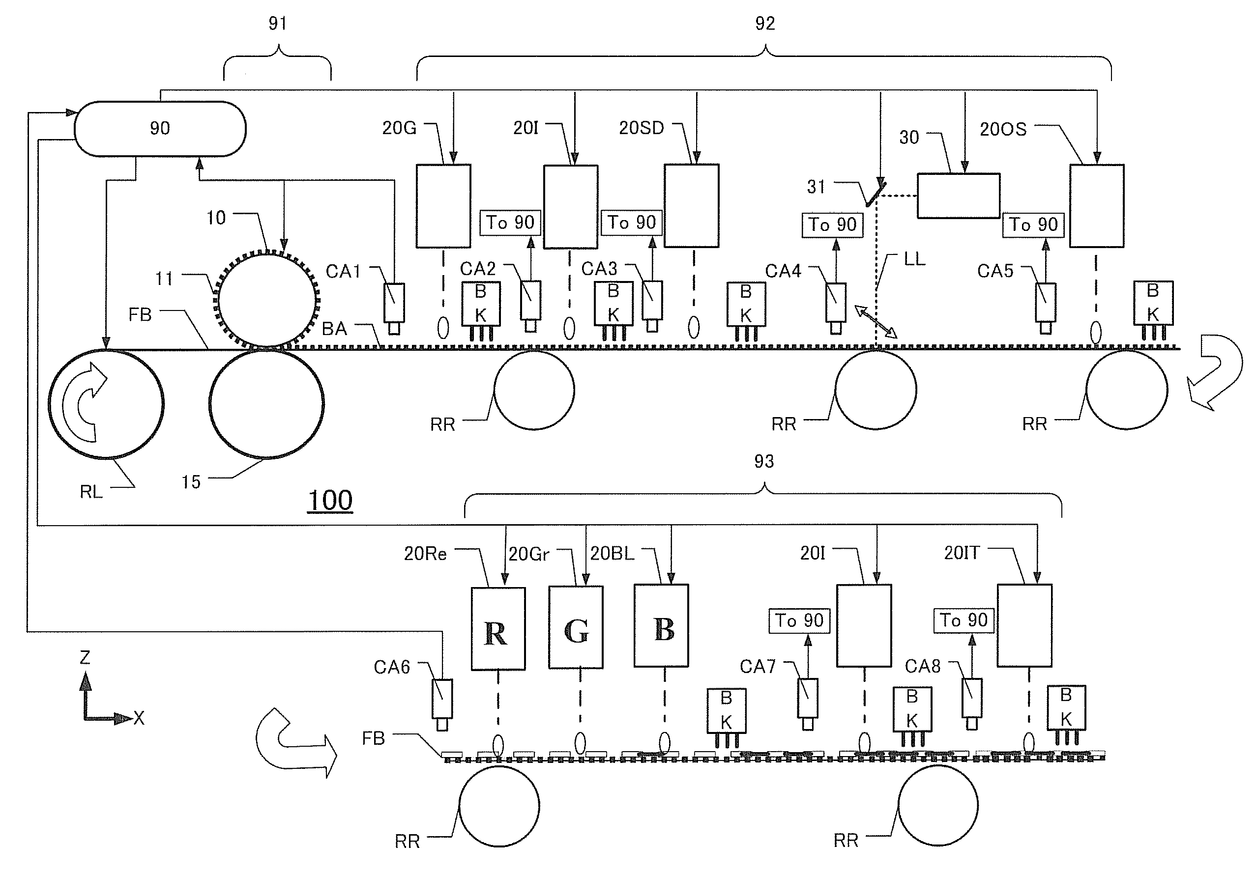
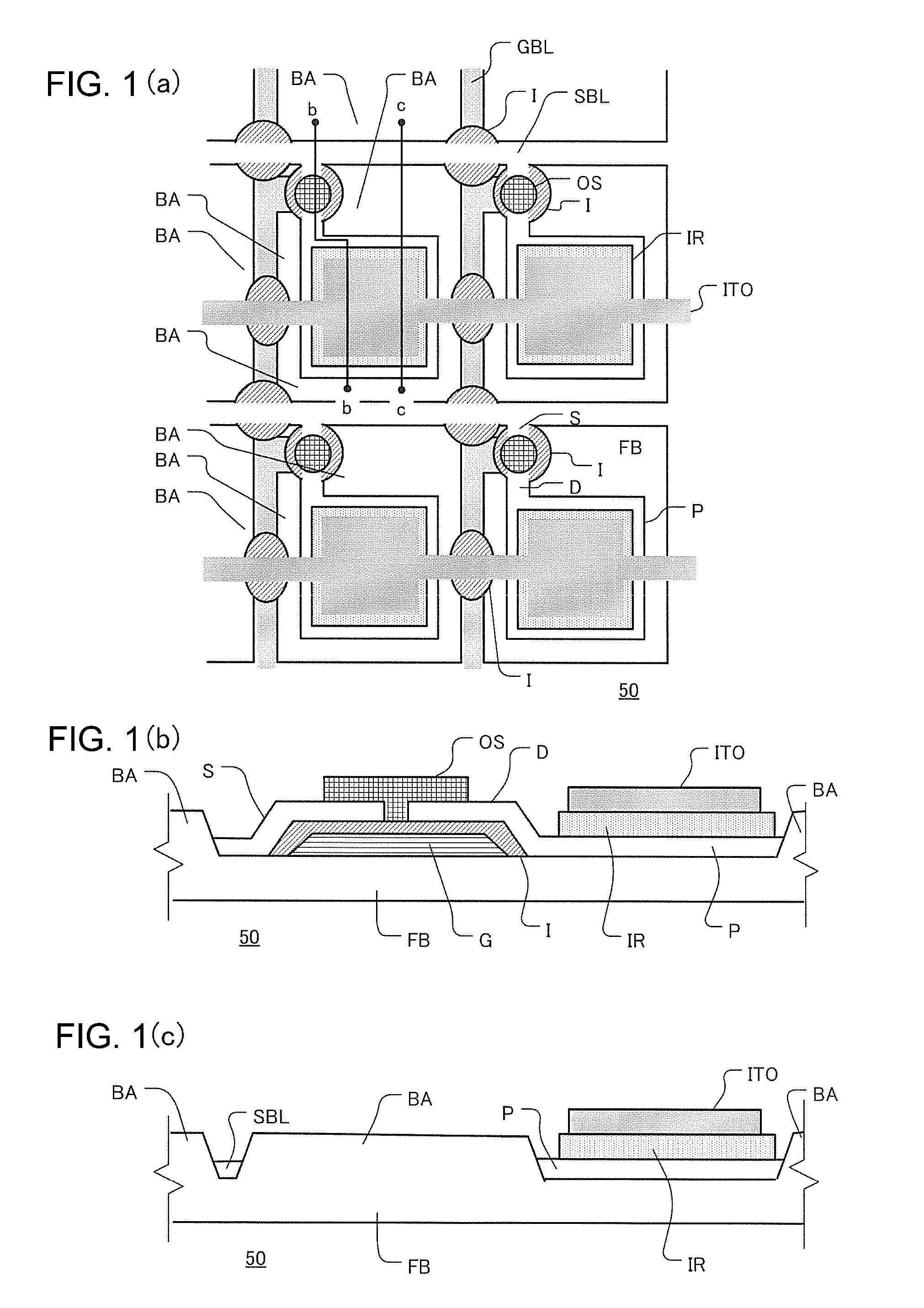
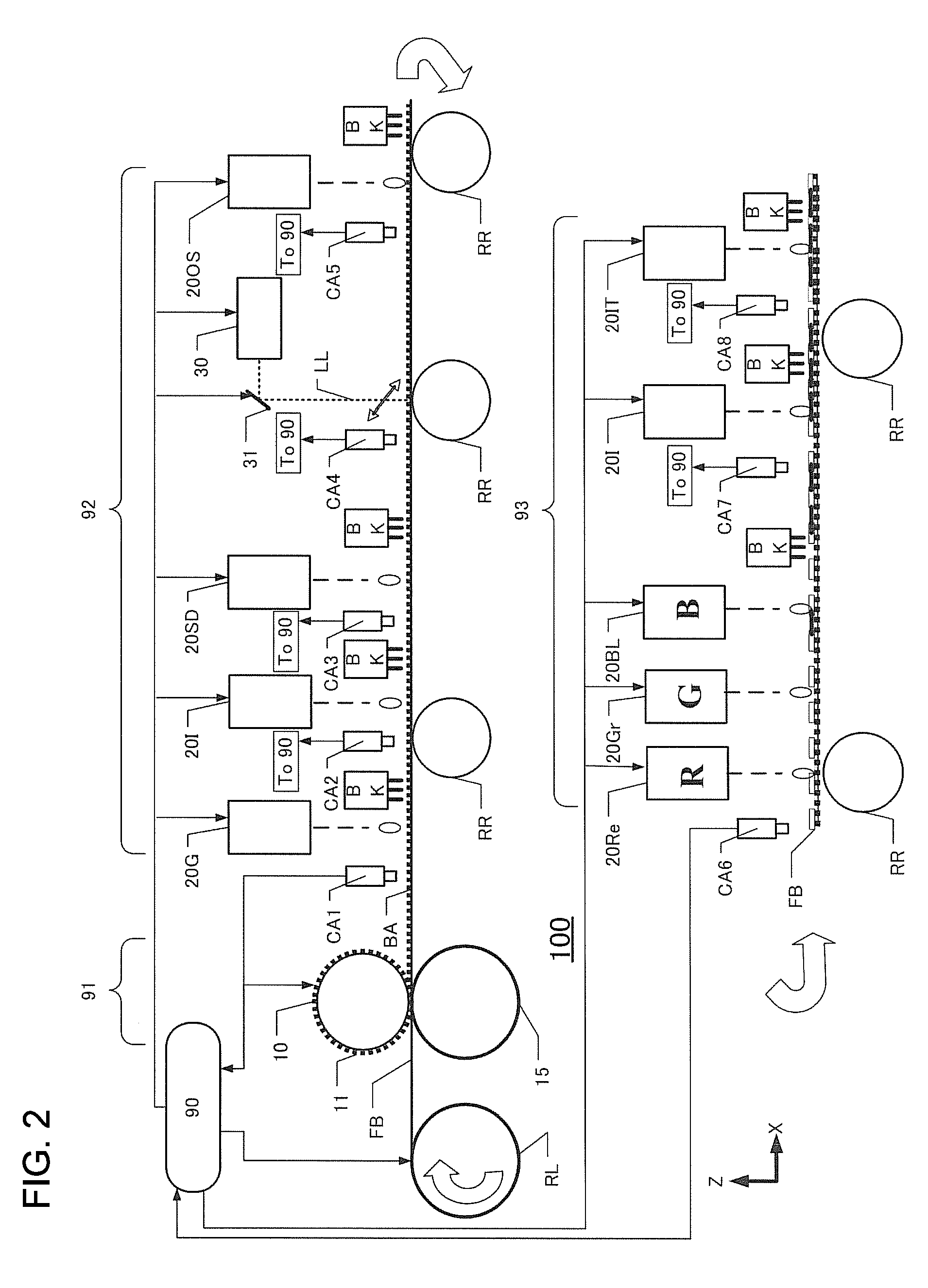
[0050]FIG. 2 is a schematic view showing a configuration of a fabrication apparatus 100 for fabricating the organic EL device 50 having the pixel electrode P and the light emitting layer IR, shown in FIG. 1(a)-(c), in the flexible sheet substrate FB.

[0051]The fabrication apparatus 100 of the organic EL device 50 of this embodiment form the sheet substrate FB in which a thin film transistor (TFT) and the pixel electrode P are formed. Further, the apparatus forms the partition wall BA in a boundary area of the pixel electrode P easily with high precision in order to precisely form one or more organic compound layers (light emitting device layers) having the light emitting layer IR on the pixel electrode P on the sheet substrate FB.

[0052]The fabrication apparatus 100 for organic EL devices is equipped with a supply roll RL for feeding a strip-shaped flexible sheet substrate FB rolled into a roll. The supply roll RL rotates at a predetermined sp...

embodiment 3

Fabrication Apparatus of Liquid Crystal Display Device

[0140]Next, a fabrication apparatus and a fabrication method of a liquid crystal display device will be described. A liquid crystal display device generally comprises a deflecting filter, a sheet substrate FB having a thin film transistor, a liquid crystal layer, a color filter, and a deflecting filter. It is explained that the sheet substrate FB having a thin film transistor among them can be formed by the fabrication apparatus 100 shown in the upper side of FIG. 2 and the fabrication apparatus 110 shown in the upper side of FIG. 9.

[0141]In Embodiment 3, supply of the liquid crystal and sticking of a color filter CF will be described.

[0142]It is generally required to supply a liquid crystal to the liquid crystal display device and also to form sealing wall for the liquid crystal. Therefore, the printing roller 40 for the partition wall formation step 91 drawn in the lower side of FIG. 9 is employed for sealing wall of the liquid...


PUM


Abstract

A method for fabricating a display device including forming a standard mark in a flexible substrate fed in a first direction, forming a partition wall in the flexible substrate, and forming an electrode by applying a conductive member at a predetermined position between the partition walls by an applicator based on the standard mark. An apparatus is provided that includes a transportation unit to transport a flexible substrate in a first direction, a mark formation unit to form a standard mark in the flexible substrate, a partition wall formation unit to form a partition wall in the flexible substrate, and an application unit to apply a conductive member to a predetermined position between the partition walls based on the standard mark. A display device is provided that includes a flexible substrate, a partition wall formed by pressing the flexible substrate, and an electrode formed by application between the partition walls.

Description

CROSS-REFERENCE TO RELATED APPLICATION[0001]The present application claims priority to Japanese Patent Application No. 2007-105464, filed Apr. 13, 2007 and U.S. Provisional Application No. 60 / 907,906, filed on Apr. 20, 2007. The contents of these applications are incorporated herein by reference in their entirety.BACKGROUND OF THE INVENTION[0002]1. Field of the Invention[0003]The present invention relates to a flat panel display device such as an organic electroluminescence device, a liquid crystal display device, or a field emission display (FED). Further, the present invention relates to a fabrication method and apparatus of the display device.[0004]2. Discussion of the Background[0005]Display devices such as liquid crystal display devices have been widely employed for various kinds of electronic appliances due to characteristics of such devices, such as compact size, thin shape, low electric power consumption, and lightweight design. Driving circuits or thin film transistors used...

Claims


Application Information

Patent Timeline
Patent Type & Authority Applications(United States)
IPC IPC(8): H01J9/24H01J9/00H01J1/62
CPCG02F1/1303G02F2001/133302G02F2001/133325H01J9/241H01L51/56H01L27/3246H01L51/0005H01L51/0022H01J9/242G02F1/133302G02F1/133325H10K59/122H10K71/135H10K71/611H10K71/40H10K71/191G02F1/1343G02F1/13H05B33/26H05B33/10H10K71/00
Inventor HAMADA, TOMOHIDENARA, KEI
Owner NIKON CORP
Learn More