
Variable device circuit and method for manufacturing the same

a variable device and manufacturing method technology, applied in variable capacitors, capacitors with electrode area variation, fixed capacitors, etc., can solve the problems of increasing the size of the device or the like, complicated drive mechanism, and difficulty in manufacturing variable capacitors, etc., to achieve stable, low-loss circuit characteristics, and manufacturing cost reduction

Inactive Publication Date: 2008-10-09
MITSUBISHI ELECTRIC CORP
View PDF7 Cites 19 Cited by
  • Summary
  • Abstract
  • Description
  • Claims
  • Application Information

AI Technical Summary

Benefits of technology

[0022]It is an object of the present invention to provide variable device circuits and method for manufacturing the same, which has stable, low-loss circuit characteristics with lower manufacturing cost by concurrent formation of variable devices and fixed passive devices, each having nearly the same device structure, on one surface of a substrate.
[0060]According to an embodiment of the present invention, concurrent formation of a variable device and a fixed passive device, each having a nearly identical device structure, by using the same manufacturing processes, can realize a variable device circuit having more stable, lower-loss circuit characteristics with lower manufacturing cost, in comparison with cases in which a variable device and a fixed passive device, each having mutually different device structures, are formed independently of each other by using different manufacturing processes.

Problems solved by technology

In this case, a complicated drive mechanism is required, and the variable capacitor is not easy to manufacture.
Also, since the radio-frequency variable capacitor has insecure factors in terms of mechanical strength, there is a need for preparing a large-sized movable beam to give enough electrostatic force to the movable beam.
This would lead to increases in size of the device or the like, entailing a problem that integration of switches, fixed capacitors, and variable inductors becomes difficult in manufacturing.
Further, although the relative variability ratio of capacitance is large, the area of the bridge as well as the distance between the bridge and the signal line of the coplanar transmission line are limited in terms of the device structure and its manufacture, so that the resultant capacitance is also limited.
As a result, it is difficult to form the bridge and the movable beam above a thick-film coplanar transmission line because of a large step gap.
This leads to an issue that conductor loss of the coplanar transmission line is hard to reduce.
This would leads to a complexity in the fabrication process.
This makes a weak point of the radio-frequency variable capacitor in terms of its manufacturing cost.
Furthermore, in a comb-tooth structure making up the fixed capacitor, there is a high possibility of short circuits between electrodes due to metallization.
It is also difficult to provide a lid structure, which is necessary to obtain stable electrical characteristics, on the rear face on which the fixed capacitor is formed.
Still more, because of the structure that has difficulty in forming a dielectric film, there is a limitation of capacitance.
Moreover, for the variable capacitor, there is a high possibility of short circuits between the upper electrode (movable electrode) and the lower electrode due to a high step gap, giving rise to a problem in operational reliability of the fixed capacitor and the variable capacitor.

Method used


Image

  • Variable device circuit and method for manufacturing the same
  • Variable device circuit and method for manufacturing the same
  • Variable device circuit and method for manufacturing the same

Examples


embodiment 1

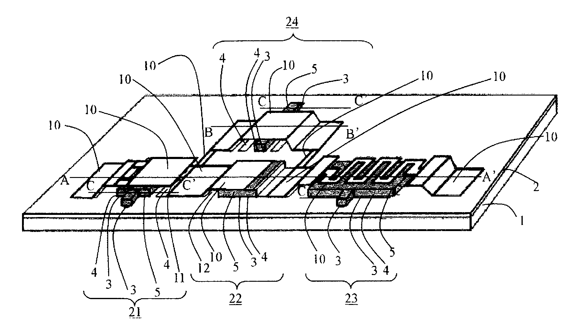
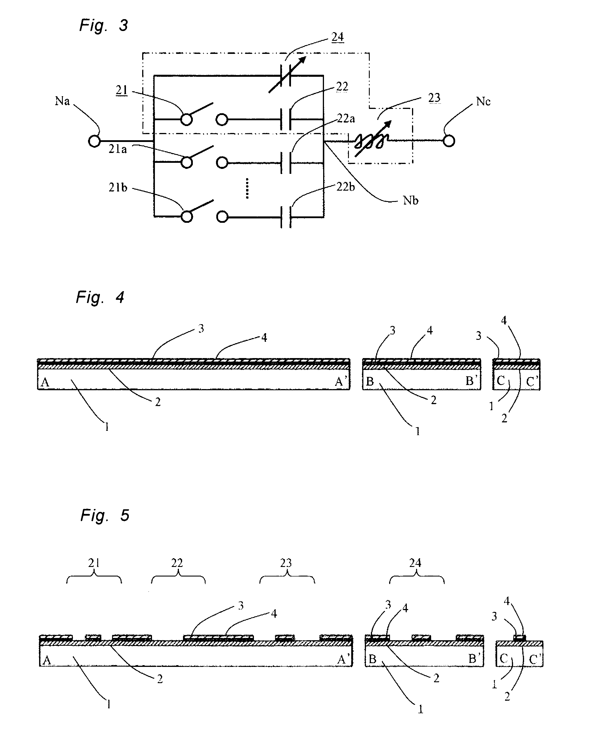
[0072]FIG. 1 is a perspective view showing an example of a variable device circuit according to Embodiment 1 of the invention. FIG. 2 shows longitudinal sectional views each taken along lines A-A′, B-B′ and C-C′ in FIG. 1. Although a radio-frequency variable component is described below, the present invention is applicable to various types of high-frequency circuits and low-frequency circuits, for example, circuits in which variable devices and fixed passive devices are integrated on one and the same substrate, and circuits in which variable devices, fixed passive devices and common semiconductor active devices are integrated on one and the same substrate.

[0073]The radio-frequency variable component includes a movable switch device 21, a fixed capacitor device 22, a variable inductor device 23, and a variable capacitor device 24, all of which are formed on the top face of a substrate 1. For easier understanding, in this case, described is an example in which each device is mounted o...

embodiment 2

[0118]FIG. 13 is a perspective view showing an example of a variable device circuit according to Embodiment 2 of the invention. FIG. 14 is a longitudinal sectional view taken along the line D-D′ in FIG. 13. FIG. 15 is a longitudinal sectional view taken along the line E-E′ in FIG. 13. This embodiment will be described below by way of an example of such a radio-frequency variable component as in Embodiment 1.

[0119]For easier understanding, in this case, described is an example in which a series circuit of the movable switch device 21 and the fixed capacitor device 22 is formed on the top face of the substrate 1. However, the movable switch device 21, the fixed capacitor device 22, the variable inductor device 23, the variable capacitor device 24 and various active devices may be mounted each in a single or plural form on the substrate 1 as in Embodiment 1.

[0120]Also, since the movable switch device 21 and the fixed capacitor device 22 are similar in construction and operation to thos...


PUM

PropertyMeasurementUnit
thickaaaaaaaaaa
resistanceaaaaaaaaaa
thicknessaaaaaaaaaa

Abstract

There is provided a variable device circuit according to the present invention, including: a substrate; at least one movable switch device formed on a first principal surface of the substrate; at least one fixed capacitor device formed on the first principal surface of the substrate; at least one variable capacitor device formed on the first principal surface of the substrate; at least one variable inductor device formed on the first principal surface of the substrate; and wiring lines for electrically connecting the devices to one another, the wiring lines being formed on the first principal surface of the substrate; wherein electrical connections among the devices can be selected by operation of the movable switch device, whereby achieving stable, low-loss circuit characteristics with lower manufacturing cost.

Description

BACKGROUND OF THE INVENTION[0001]1. Field of the Invention[0002]The present invention relates to variable device circuits and method for manufacturing the same, which can be formed by applying micromachining techniques or the like and which is suitable for radio-frequency variable components to be used in radio-frequency bands such as microwaves, semi-millimeter waves and millimeter waves.[0003]2. Description of the Related Art[0004]Recently, radio-frequency devices using micromachining techniques, so called RFMEMS (Radio Frequency Micro-Electro-Mechanical-Systems) devices, have been drawing attention. With this technique, high-aspect three-dimensional structures, hollow structures, variable structures and the like can be easily manufactured, thereby expectably allowing radio-frequency devices and circuits to be fabricated on low-priced silicon substrates with low cost, low loss, high isolation, and high-performance.[0005]Also recently, RFMEMS radio-frequency variable circuits made ...

Claims


Application Information

Patent Timeline
Patent Type & Authority Applications(United States)
IPC IPC(8): H01G7/00H05K7/02H05K3/30H01G4/00
CPCH01G5/16H01G5/40H01L27/016H01L27/13Y10T29/4913H03H2001/0064H03H2007/008H03H7/175H03H7/0115
Inventor LEE, SANGSEOKYOSHIDA, YUKIHISANISHINO, TAMOTSUINOUE, HIROMOTOSODA, SHINNOSUKEMIYAZAKI, MORIYASU
Owner MITSUBISHI ELECTRIC CORP
Learn More