
Aligning device, bonding apparatus, and aligning method

a bonding apparatus and aligning device technology, applied in auxillary welding devices, program control, instruments, etc., can solve problems such as difficulty in precisely recognizing both marks, unable to disclose an optical system for aligning, and unable to achieve alignment reliably. , to achieve the effect of aligning

Inactive Publication Date: 2008-10-09
MURATA MFG CO LTD
View PDF3 Cites 33 Cited by
  • Summary
  • Abstract
  • Description
  • Claims
  • Application Information

AI Technical Summary

Benefits of technology

[0011]Accordingly, in view of the above-described circumstances, it is desired to provide an aligning device that can reliably correct misalignment between electronic components and can increase the accuracy in aligning the electronic components, a bonding apparatus equipped with the aligning device, and an aligning method.

Problems solved by technology

Moreover, since the elastic material is provided between the lower surface plate and the upper surface plate, it is difficult to precisely recognize both marks.
Since the above-described Patent Document 2 is originally not intended to align and bond two electronic components, it does not disclose an optical system for alignment.
If a camera is placed below the sample stage, problems similar to those in the above-described Patent Document 2 arise.
Further, it is physically difficult to insert an optical system in a cutout provided in the flexible cylindrical member, because deformation of the cylindrical member imposes load on the optical system.

Method used


Image

  • Aligning device, bonding apparatus, and aligning method
  • Aligning device, bonding apparatus, and aligning method
  • Aligning device, bonding apparatus, and aligning method

Examples


Embodiment Construction

Reference Numerals

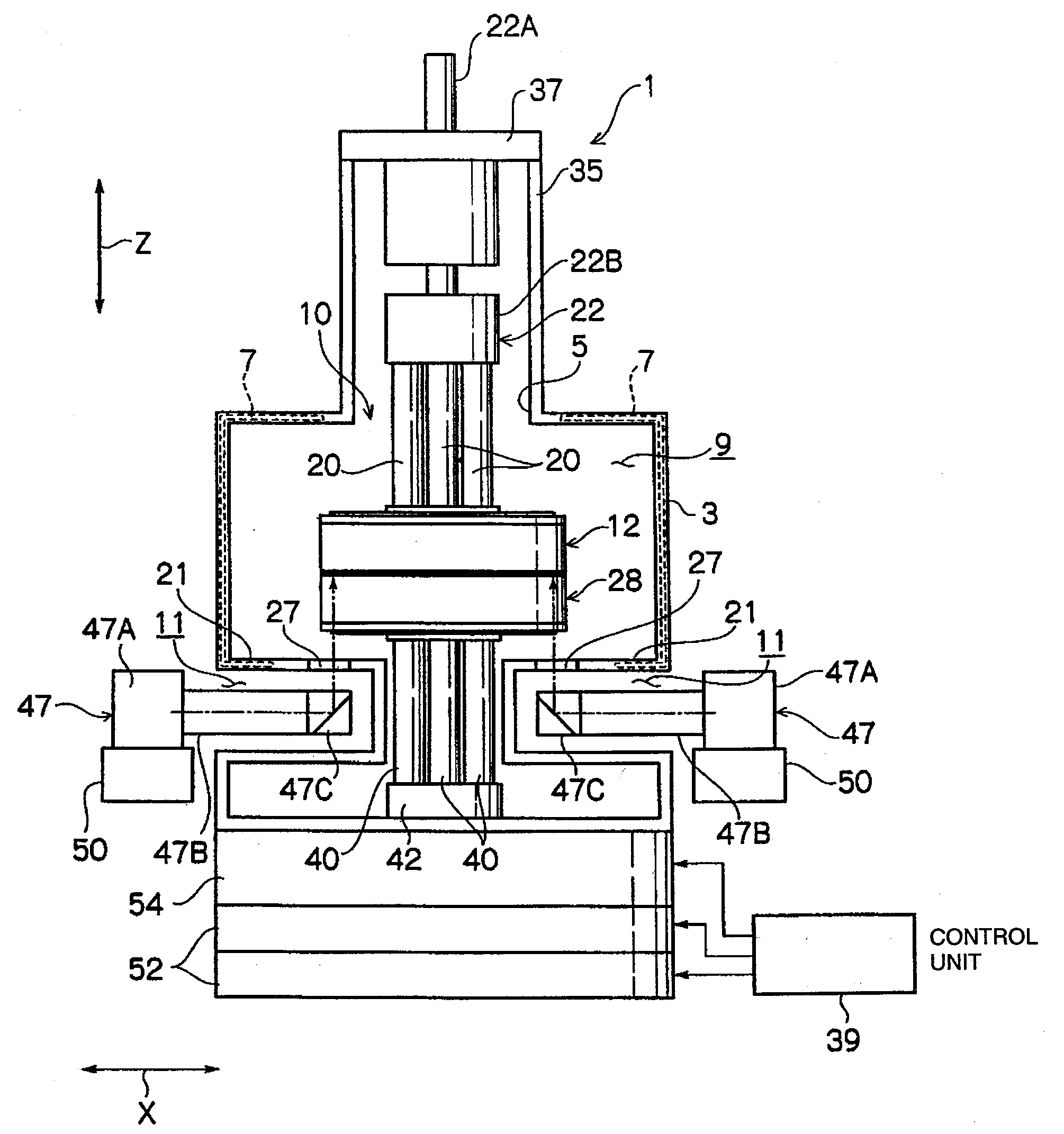
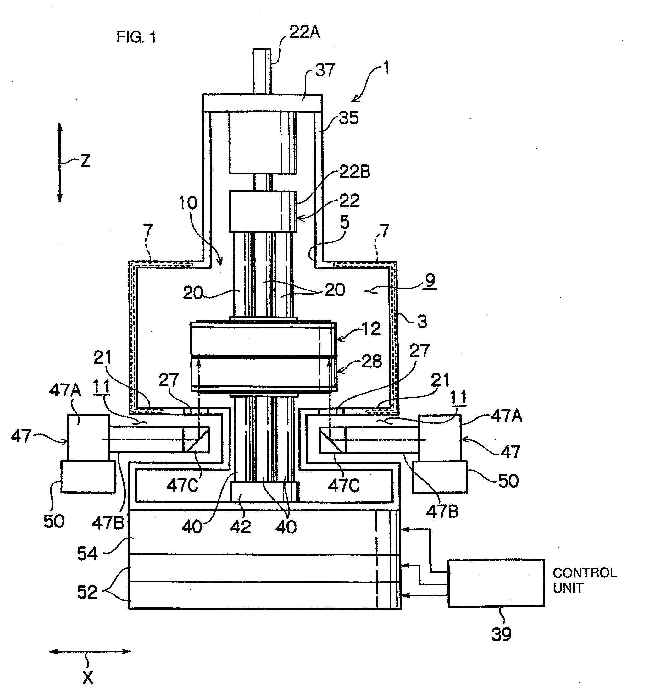
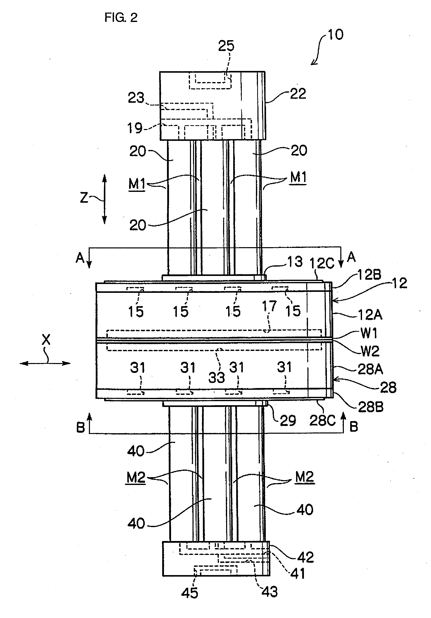
[0084]1: aligning device[0085]3: chamber[0086]7: cooling-water channel[0087]9: airtight chamber[0088]10: bonding apparatus[0089]11: space[0090]12: first block member[0091]12A: first presser plate[0092]12B: first back plate[0093]12C: first heater chip (heating member, heater chip)[0094]15: first cooling groove (first cooling-gas channel)[0095]17: first drawing groove[0096]19: first N2-gas supply (first cooling-gas supply channel)[0097]20: first column members (first flexible member)[0098]21: image-taking port[0099]22: first pressure shaft (first pressure member)[0100]23: first air channel[0101]24: first hollow member (first hollow duct)[0102]25: first cooling-fluid circulation path[0103]26: first O-ring (first elastic member)[0104]27: observation window[0105]28: second block member[0106]28A: second presser plate[0107]28B: second back plate[0108]28C: second heater chip (heating member, heater chip)[0109]31: second cooling groove (second cooling-gas channel)[0110]33: ...


PUM

PropertyMeasurementUnit
flexibleaaaaaaaaaa
distanceaaaaaaaaaa
pressureaaaaaaaaaa

Abstract

An aligning device that can reliably correct misalignment between electronic components for increasing the accuracy in aligning the electronic components, a bonding apparatus equipped with the aligning device, and an aligning method. The aligning device comprises a chamber; a flexible bellows configured to define an airtight chamber therein with the chamber; a driving unit configured to move one of a first block member and a second block member relative to the other, the first block member being for holding a first electronic component and being provided in the airtight chamber, and the second block member being for holding a second electronic component and being provided in the airtight chamber; and an image-taking port protruding inward from an outer surface of the chamber so as to define a space, the image-taking port having an observation window through which at least one of the first electronic component and the second electronic component is observed. In an embodiment, an image-taking port 21 protrudes inward from an outer surface of a chamber 3 so as to define a space 11. Thus, even when the chamber 3 moves together with a second block-member 28, an image recognizing device 47 can be provided in the space 11 so as to be prevented from interfering with the motion of the chamber 3. This allows the chamber 3 to freely move without any restriction. As a result, one of a first block member 12 and the second block member 28 can be freely moved relative to the other without being restricted by the placement of the image recognizing device 47, and a first wafer W1 and a second wafer W2 can be aligned reliably.

Description

CROSS-REFERENCE TO RELATED APPLICATIONS[0001]This is a continuation under 35 U.S.C. §111(a) of PCT / JP2006 / 317467 filed Sep. 4, 2006, and claims priority of JP2005-357955 filed Dec. 12, 2005, incorporated by reference.BACKGROUND[0002]1. Technical Field[0003]The present disclosure relates to an aligning device for precisely aligning electronic components such as wafers, a bonding apparatus equipped with the aligning device, and an aligning method.[0004]2. Background Art[0005]In a known method for bonding liquid crystal substrates, an upper surface plate, on which an upper substrate having a positioning mark is held, and a lower surface plate, on which a lower substrate similarly having a positioning mark is held, with an elastic material disposed between the upper and lower surface plates, are stored to face each other in a vacuum chamber. The positions of the marks on the upper and lower substrates are recognized, and an absolute difference between the positions is recognized. When i...

Claims


Application Information

Patent Timeline
Patent Type & Authority Applications(United States)
IPC IPC(8): H05K3/30G02F1/13
CPCB32B37/0046B32B38/1833B32B2305/55B32B2309/68B32B2309/70B32B2457/14Y10T29/53174H01L21/682Y10T29/53178Y10T156/1075Y10T29/53183Y10T29/49131Y10T29/5313G02F2001/133354G02F1/133354G05B19/402G05B2219/37608H01L21/681
Inventor HIRATA, ATSUHIKOFUKUNAGA, SHIGEKIYAMANE, SHIGEKINAMURA, MITSUHIROSUZUKI, ARATAWATANABE, TOMONARI
Owner MURATA MFG CO LTD
Learn More