Liquid crystal display element and method for manufacturing the same
a technology of liquid crystal display element and liquid crystal, which is applied in non-linear optics, instruments, optics, etc., can solve the problem of not easy to detect the just etching timing, and achieve the effect of improving the opening area ratio of array board, increasing the luminescence variation amount of etching gas during dry etching, and easy detection
- Summary
- Abstract
- Description
- Claims
- Application Information
AI Technical Summary
Benefits of technology
Problems solved by technology
Method used
Image

Examples
first embodiment
[0020]The construction of a liquid crystal display element of the present invention will now be described with reference to FIG. 1 to FIG. 7.
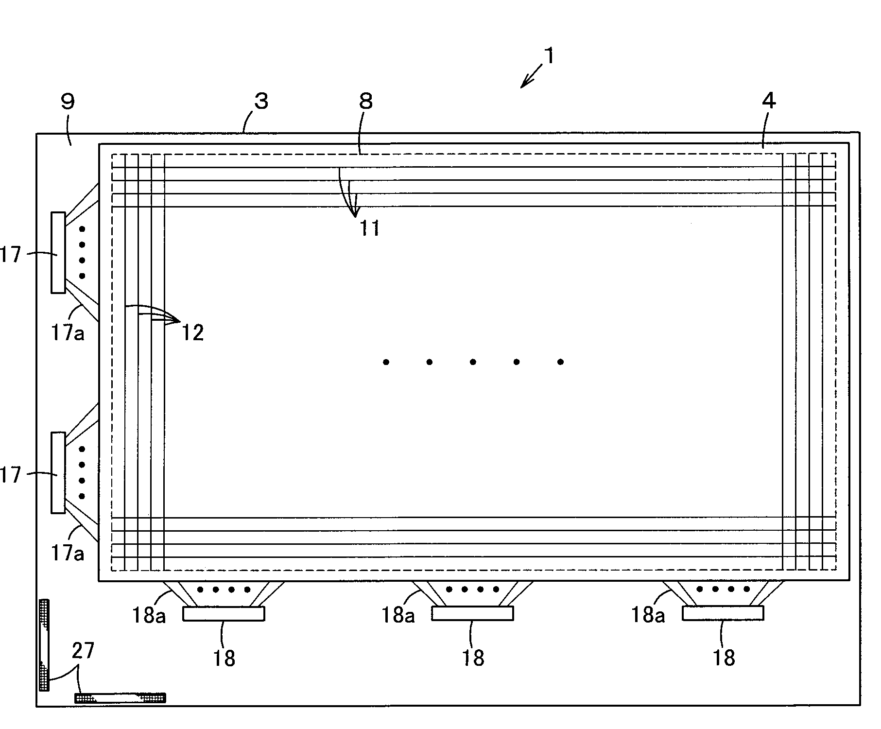
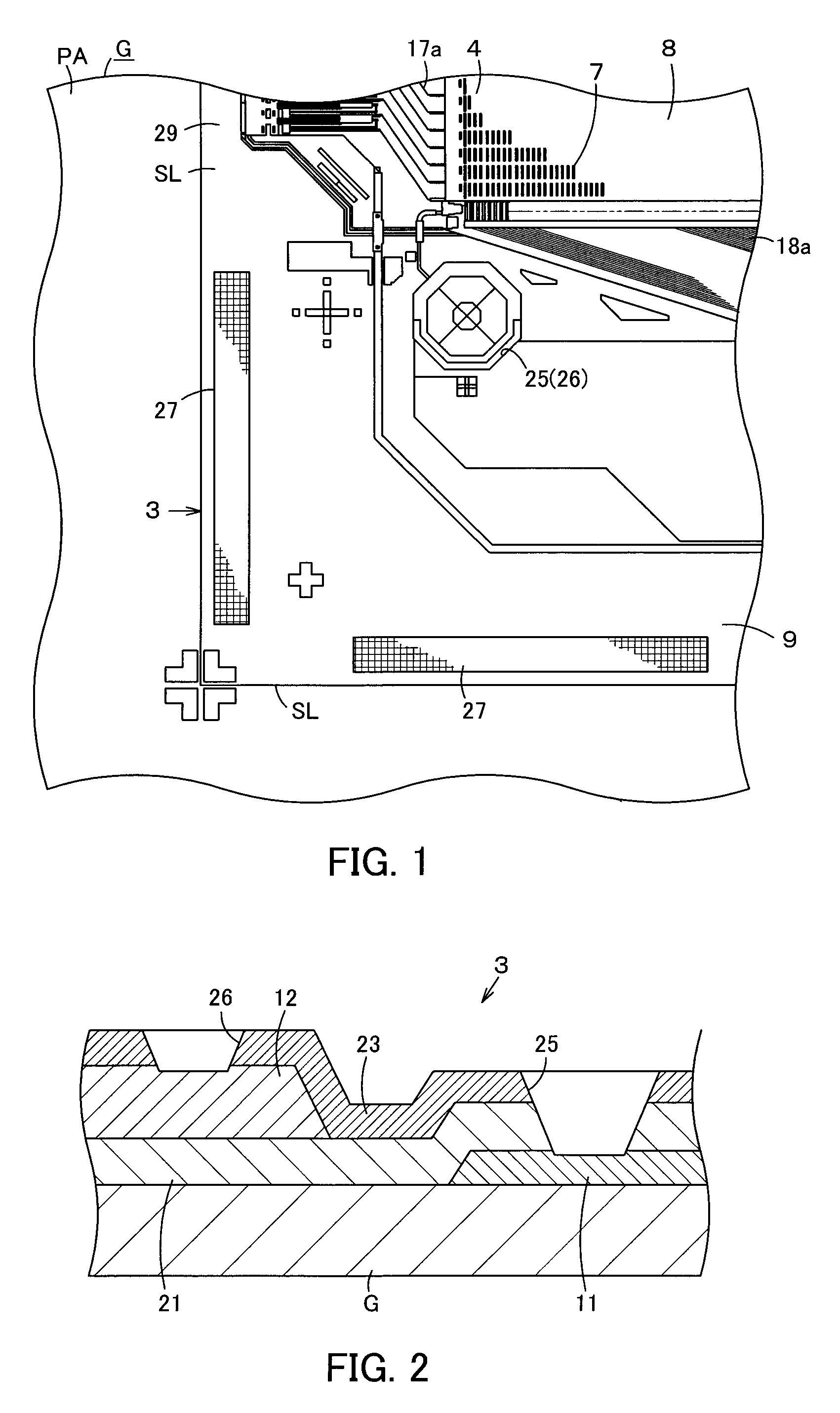
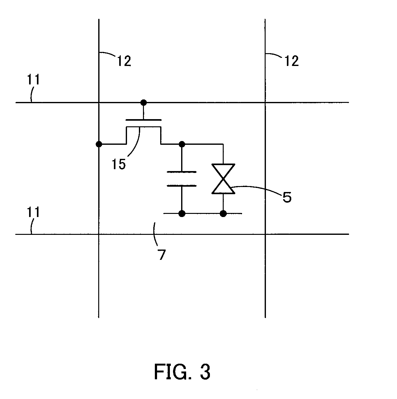
[0021]In FIG. 4, reference numeral 1 represents an active matrix type liquid crystal panel as a liquid crystal display element. The liquid crystal panel 1 includes an array board 3, a counter board 4, a liquid crystal layer 5 sandwiched between the array board 3 and the counter board 4. The array board 3 and the counter board 4 of the liquid crystal panel 1 are adhesively attached to each other by a sealing agent S while the liquid crystal layer 5 is held between the array board 3 and the counter board 4. Polarization plates (not shown) are arranged on the respective outer surfaces at the outside of the array board 3 and the counter board 4 so that the polarization axes thereof are perpendicular to each other. Furthermore, as shown in FIG. 1, a planar rectangular display region 8 which has a plurality of pixels 7 arranged in a matrix form and c...
second embodiment
[0052]In the second embodiment, the dummy holes 27 are provided out of the parting lines, that is, the scribe lines SL of the respective glass boards G of the large-sized mother board 29.
[0053]That is, the dummy holes 27 are not formed on each liquid crystal panel 1, but formed on the end member portion PA which is cut out from the scribe line SL.
[0054]In this case, the opening area ratio is secured by the dummy holes 27, whereby the same effect as the first embodiment can be attained. In addition, the end member portion PA is cut out and thus it does not constitute a part of the liquid crystal panel 1, so that the dummy holes 27 can be easily formed without strict consideration of the surrounding arrangement, etc.
[0055]In each of the above embodiments, any position such as the non-display region 9, the outside of the scribe line SL or the like may be set as the position of the dummy hole 27 insofar as it hardly affects the display region 8.
[0056]Furthermore, the details of the liqu...
PUM
| Property | Measurement | Unit |
|---|---|---|
| thickness | aaaaa | aaaaa |
| thickness | aaaaa | aaaaa |
| opening area ratio | aaaaa | aaaaa |
Abstract
Description
Claims
Application Information
 - R&D
- Intellectual Property
- Life Sciences
- Materials
- Tech Scout
- Unparalleled Data Quality
- Higher Quality Content
- 60% Fewer Hallucinations
Browse by: Latest US Patents, China's latest patents, Technical Efficacy Thesaurus, Application Domain, Technology Topic, Popular Technical Reports.
© 2025 PatSnap. All rights reserved.Legal|Privacy policy|Modern Slavery Act Transparency Statement|Sitemap|About US| Contact US: help@patsnap.com