Self-luminous device

Inactive Publication Date: 2008-07-24
STANLEY ELECTRIC CO LTD
View PDF10 Cites 73 Cited by
  • Summary
  • Abstract
  • Description
  • Claims
  • Application Information

AI Technical Summary

Benefits of technology

[0012]In view of the foregoing, it is an object of the present invention to effectively extract the light emitted from the illuminants used in self-luminous devices into the air.
[0013]It is another object to improve the light extraction efficiency of self-luminous devices without requiring elaborate processes.
[0014]It is still another object of the present invention to improve the light extraction efficiency of self-luminous devices having a periodic structure with imperfect periodicity.

Problems solved by technology

One drawback of these devices is that the efficiency of light utilization is low since the light emitted from the illuminants is not effectively extracted outside due to the total internal reflection.
One problem of the periodic structure approach is that the structure may not be made with perfect periodicity depending on the type of the process used to make it.
Such defective periodic structures cannot achieve sufficiently high light extraction efficiency.
However, the quality of the light emitting layer is significantly affected by the integration of the diffraction grating, making this approach impractical.

Method used


Image

  • Self-luminous device
  • Self-luminous device
  • Self-luminous device

Examples


first embodiment

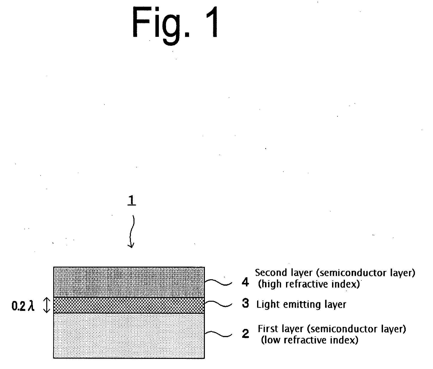
[0064]As in the first embodiment, the semiconductor layers 2, 4 and the light emitting layer 3 together form the self-luminous device 1. In one construction, each of the first semiconductor layer 2 and the second semiconductor layer 4 may be formed as a cladding layer made of AlGaN and the light emitting layer 3 may be made of InGaN.

[0065]The distribution of refractive indices of the first semiconductor layer 2, the light emitting layer 3 and the second semiconductor layer 4 may be either asymmetric as in the first embodiment, or symmetric. In the asymmetric construction, the light emitting layer 3, the first semiconductor layer 2 (cladding layer of AlGaN) and the second semiconductor layer 4 (cladding layer of AlGaN) may have refractive indices of, for example, 2.8, 2.5 and 2.78, respectively. In the symmetric construction, the light emitting layer 3 may have a refractive index of, for example, 2.8 while the first semiconductor layer 2 (cladding layer of AlGaN) and the second semic...

second embodiment

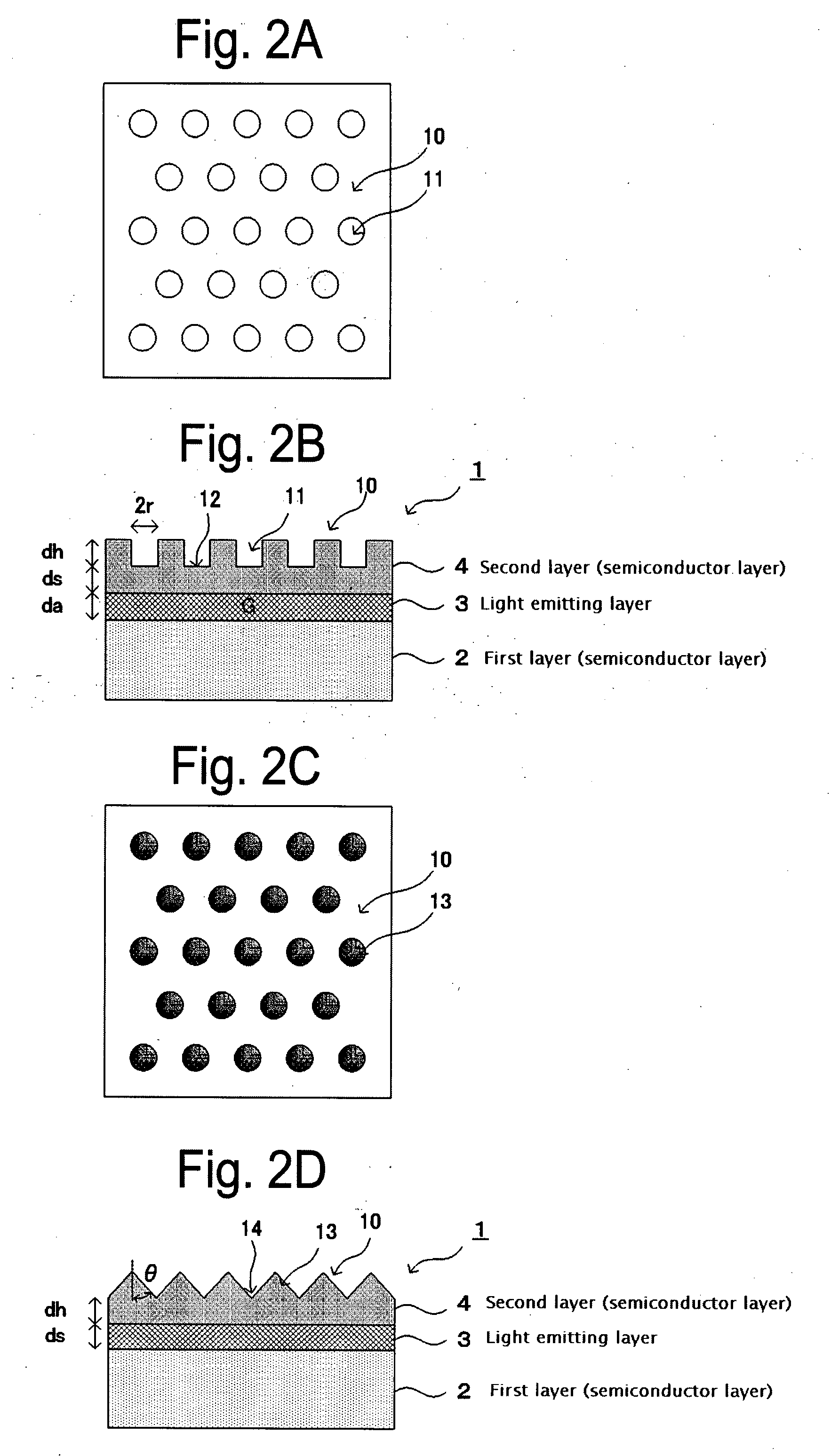
[0066]In the second embodiment, the two-dimensional periodic structure 10 may be a dense array of circular pores or a dense array of cone-shaped projections and may be formed of photonic crystals or photonic quasicrystals. Cone-shaped projections such as conical projections, pyramidal projections or projections of any desired shape may be densely arrayed to form the dense array of cone-shaped projections.

[0067]The photonic crystals are formed by arranging regions of different refractive indices in a repetitive pattern with a period substantially equal to the wavelength of light. The photonic quasicrystals are formed by arranging, in accordance with a repetitive quasicrystal pattern, patterns of photonic crystals that have two types of regions having two different refractive indices in which the two regions alternately repeat with a period substantially equal to the wavelength of light. The photonic quasicrystals have a quasiperiodic structure of refractive index that does not have t...

third embodiment

[0087]the present invention is now described with reference to FIG. 4.

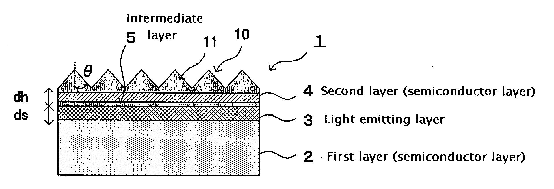
[0088]Referring to FIG. 4, a self-luminous device 1 of the third embodiment is shown. As in the first embodiment, the self-luminous device of the third embodiment improves the light extraction efficiency by optimizing the distribution of refractive index in the semiconductor layers that form the self-luminous device. This embodiment is characterized by its multilayer structure including an intermediate layer.

[0089]The self-luminous device 1 has a multilayer structure comprising a first semiconductor layer 2, a light emitting layer 3 overlaying the first semiconductor layer 2, a second semiconductor layer 4 overlaying the light emitting layer 3, and an intermediate layer 5 within the second semiconductor layer 4.

[0090]A first form of the intermediate layer 5 has a refractive index close to that of the light emitting layer 3 and is formed of a medium that does not absorb the light emitted from the light emitting lay...


PUM


Abstract

A self-luminous device 1 is one embodiment which has an increased light extraction efficiency by optimizing the distribution of refractive index in semiconductor layers. The self-luminous device 1 includes a first layer (semiconductor layer 2), a light emitting layer 3 overlaying the first layer (semiconductor layer 2), and a second layer (semiconductor layer 4) overlaying the light emitting layer 3. The first layer (semiconductor layer 2) and the second layer (semiconductor layer 4) have different refractive indices so that the refractive indices of the two layers (semiconductor layers 2 and 4) are asymmetric with respect to the light emitting layer interposed therebetween. In the refractive index distribution of asymmetric layers (semiconductor layers), the refractive index of the second layer (semiconductor layer 4) is higher than that of the first layer (semiconductor layer 2).

Description

CROSS-REFERENCE TO RELATED APPLICATIONS[0001]This application is a Continuation Application of International Application PCT / JP2006 / 305167, filed Mar. 15, 2006, which is incorporated by reference herein.[0002]This application claims the benefit of priority under 35 USC 119 of Japanese Patent Applications No. 2005-092412 filed on Mar. 28, 2005, and No. 2005-204976 filed on Jul. 13, 2005, which are incorporated by reference herein.BACKGROUND OF THE INVENTION[0003]1. Field of the Invention[0004]The present invention relates to self-luminous devices, such as light emitting diodes (LEDs) and organic electroluminescent (EL) devices.[0005]2. Description of the Related Art[0006]Self-luminous devices, such as light emitting diodes (LEDs) and organic electroluminescent (EL) devices, are expected to be used in a wide range of applications, including signs, displays and illuminations. One drawback of these devices is that the efficiency of light utilization is low since the light emitted from t...

Claims


Application Information

Patent Timeline
IPC IPC(8): H01L33/00H01L33/32
CPCH01L33/20H01L2933/0083H01L33/44
Inventor BABA, TOSHIHIKOMORITO, KOSUKE
Owner STANLEY ELECTRIC CO LTD
Why Eureka
Try Eureka