Systems for displaying images by utilizing vertical shift register circuit to generate non-overlapped output signals
a vertical shift register and output signal technology, applied in the field of display images, can solve problems such as increased power consumption, and achieve the effect of reducing production costs and power consumption
- Summary
- Abstract
- Description
- Claims
- Application Information
AI Technical Summary
Benefits of technology
Problems solved by technology
Method used
Image
Examples
first embodiment
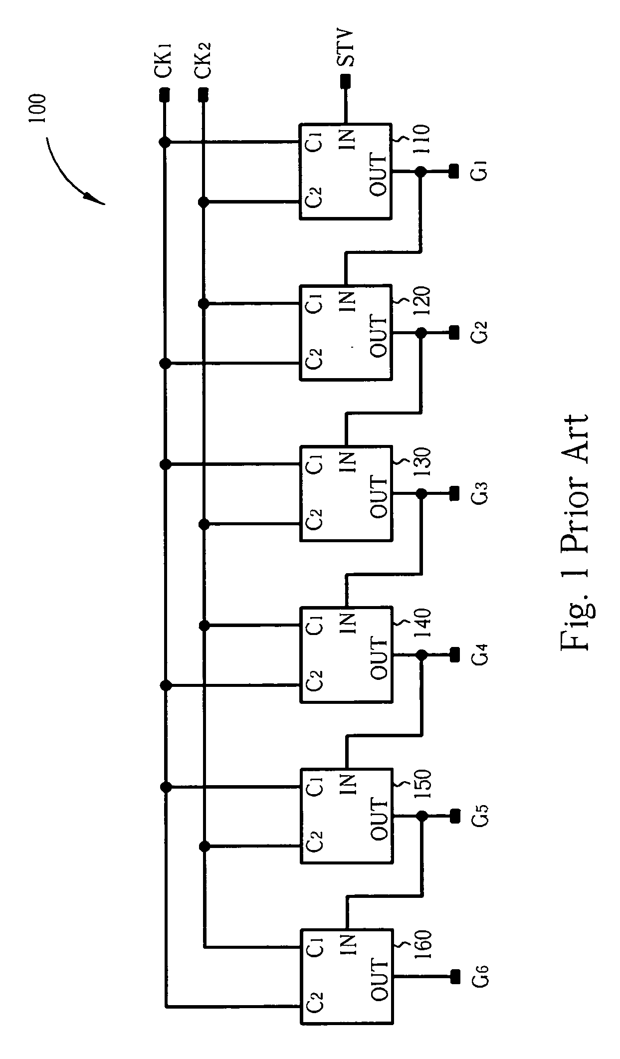
[0034]Please refer to FIG. 6. FIG. 6 is a block diagram illustrating a dynamic shift register 600 according to the present invention. As shown in FIG. 6, the dynamic shift register 600 includes a sampling circuit 620, a holding unit 630, and a first logic circuit 650. In this embodiment, the sampling circuit 620 samples an incoming signal Sin inputted at an input terminal In2 according to a clock signal CK1 received from an input terminal In1; the holding unit 630 then holds the sampled value, generated from the preceding sampling circuit; and the first logic circuit 650 finally outputs an output signals So to an output terminal OUT by referencing the held sampled value and a clock signal CK2 inputted at an input terminal In2. Please note, an additional output terminal NXT coupled to the output of the holding circuit 630 is created in the dynamic shift register 600 for further utilization, which is detailed later.
[0035]Please refer to FIG. 7. FIG. 7 is a circuit diagram illustrating...
second embodiment
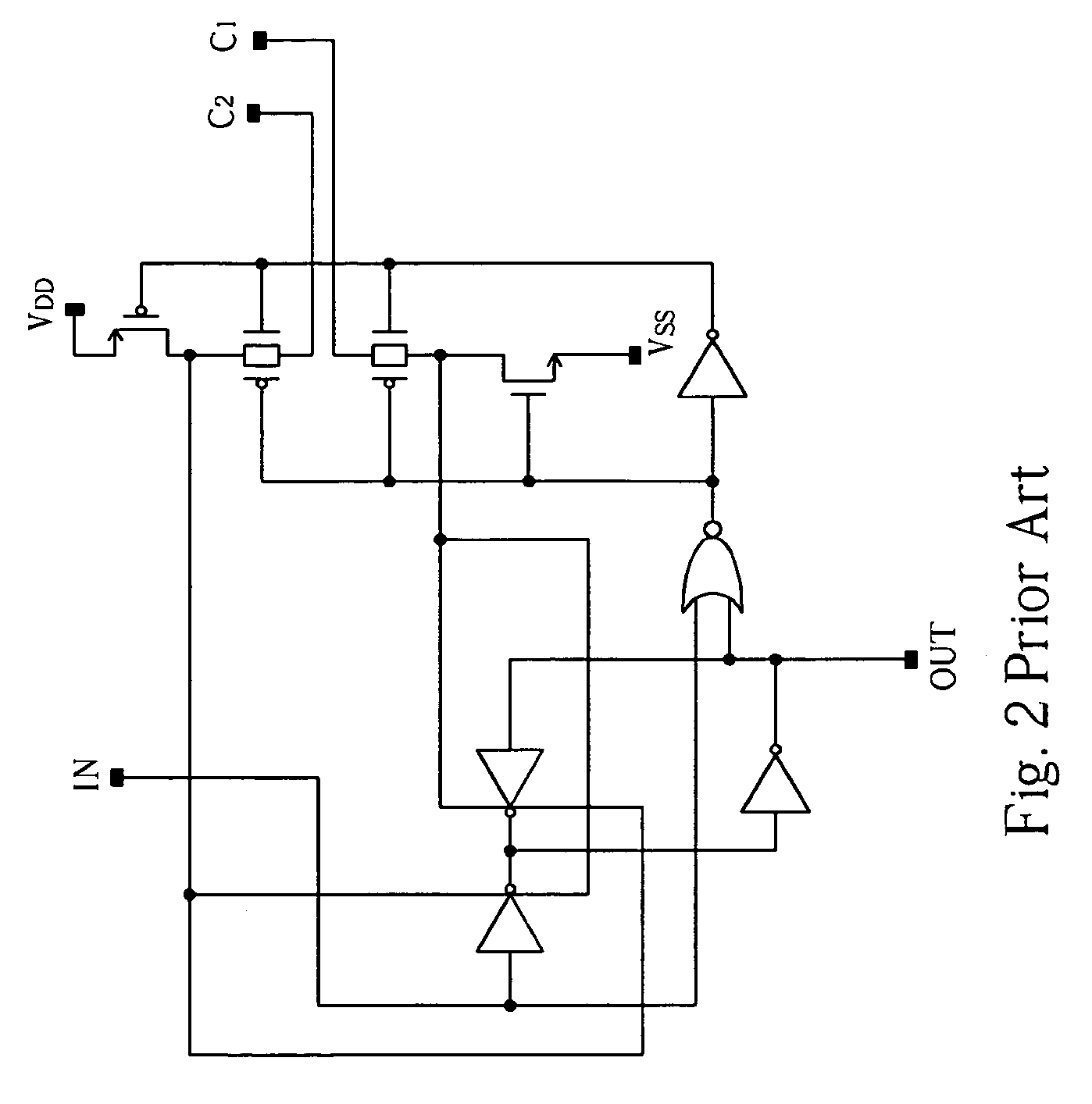
[0037]Please refer to FIG. 9. FIG. 9 is a circuit diagram illustrating the dynamic shift register 600 shown in FIG. 6. The circuitry shown in FIG. 9 is similar to that shown in FIG. 7. The major difference is the configuration of the first logic circuit 650. In this embodiment, the first logic circuit 650 includes a first switching circuit 910, a second switching circuit 920, and an inverter 930. The first switching circuit 910 comprises an N-MOSEFT 912 and a P-MOSFET 914, which are connected in parallel and both receiving the clock signal CK2 at the source terminal and generating an output signal at the drain terminal. The second switching circuit 920 is implemented by an N-MOSFET 922. Both the first switching circuit 910 and the second switching circuit 920 are controlled by the voltage level held by the holding circuit 630. More specifically, when the held voltage level is at a high level, the voltage level at the node NR will be opposite to the high level, i.e., a low level, due...
third embodiment
[0042]However, the confirmation of the second logic circuit 1010 shown in FIG. 11 or FIG. 12 has an inherent leakage problem caused by the P-MOSFET 1012. Referring to FIG. 8, the clock signal CK1 has a transition from a high level to a low level at t2, turning off the N-MOSFET 1016 in conjunction with the N-MOSFET 1022. However, the input signal at the input terminal In3, having the waveform as that of the input signal Sin shown in FIG. 8, has a transition from a high level to a low level at t3. In addition, the input clock CK2 has a transition from a low level to a high level at the same time (i.e., t3) to make the output signal So has an identical transition since the voltage level held by the holding circuit 1030 is at a low level. However, the low level at the input terminal In3 will make the P-MOSFET 1012 enable a leakage path that might affect the currently held voltage level (i.e., a low level) in the holding circuit 1030. In a worst case, erroneous output signal is outputted...
PUM
 Abstract
Description
Claims
Application Information
 - R&D
- Intellectual Property
- Life Sciences
- Materials
- Tech Scout
- Unparalleled Data Quality
- Higher Quality Content
- 60% Fewer Hallucinations
Browse by: Latest US Patents, China's latest patents, Technical Efficacy Thesaurus, Application Domain, Technology Topic, Popular Technical Reports.
© 2025 PatSnap. All rights reserved.Legal|Privacy policy|Modern Slavery Act Transparency Statement|Sitemap|About US| Contact US: help@patsnap.com


