Organic field effect transistor and semiconductor device
a field effect transistor and organic semiconductor technology, applied in the field of field effect transistors, can solve the problems of low chemical stability of conductivity imparting agents, difficult substrate plastics or films, and limited organic semiconductor materials, etc., to achieve excellent adhesion with a semiconductor layer, reduce energy barriers, and expand the range of choice
- Summary
- Abstract
- Description
- Claims
- Application Information
AI Technical Summary
Benefits of technology
Problems solved by technology
Method used
Image
Examples
embodiment mode 1
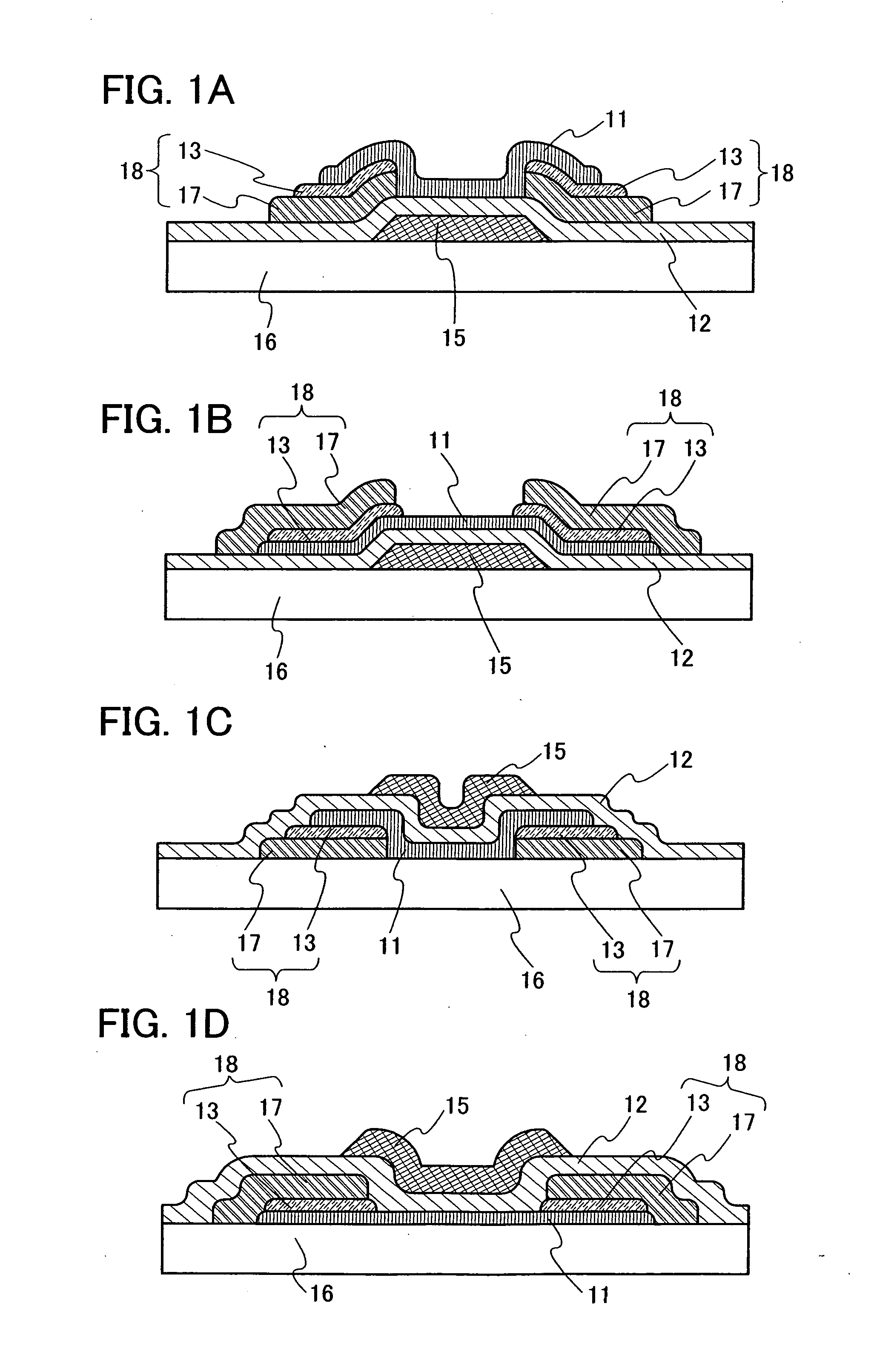
[0115]FIGS. 1A to 1D each show a structural example of an organic field effect transistor of the present invention. In the drawings, reference numeral 11 denotes a semiconductor layer containing an organic semiconductor material; 12, an insulating layer; 13, a composite layer; 15, a gate electrode; and 16, a substrate. A source electrode and a drain electrode 18 each include the composite layer 13 and a conductive layer 17. Arrangement of each layer or each electrode can be appropriately selected depending on the usage of an element. In addition, in the drawings, the composite layer 13 is provided so as to be in contact with the semiconductor layer 11; however, the present invention is not limited thereto. The composite layer 13 may be included in part of the source electrode and / or the drain electrode. It is to be noted that arrangement of each layer or each electrode can be appropriately selected from FIGS. 1A to 1D depending on the usage of the element.
[0116]As the substrate 16, ...
embodiment mode 2
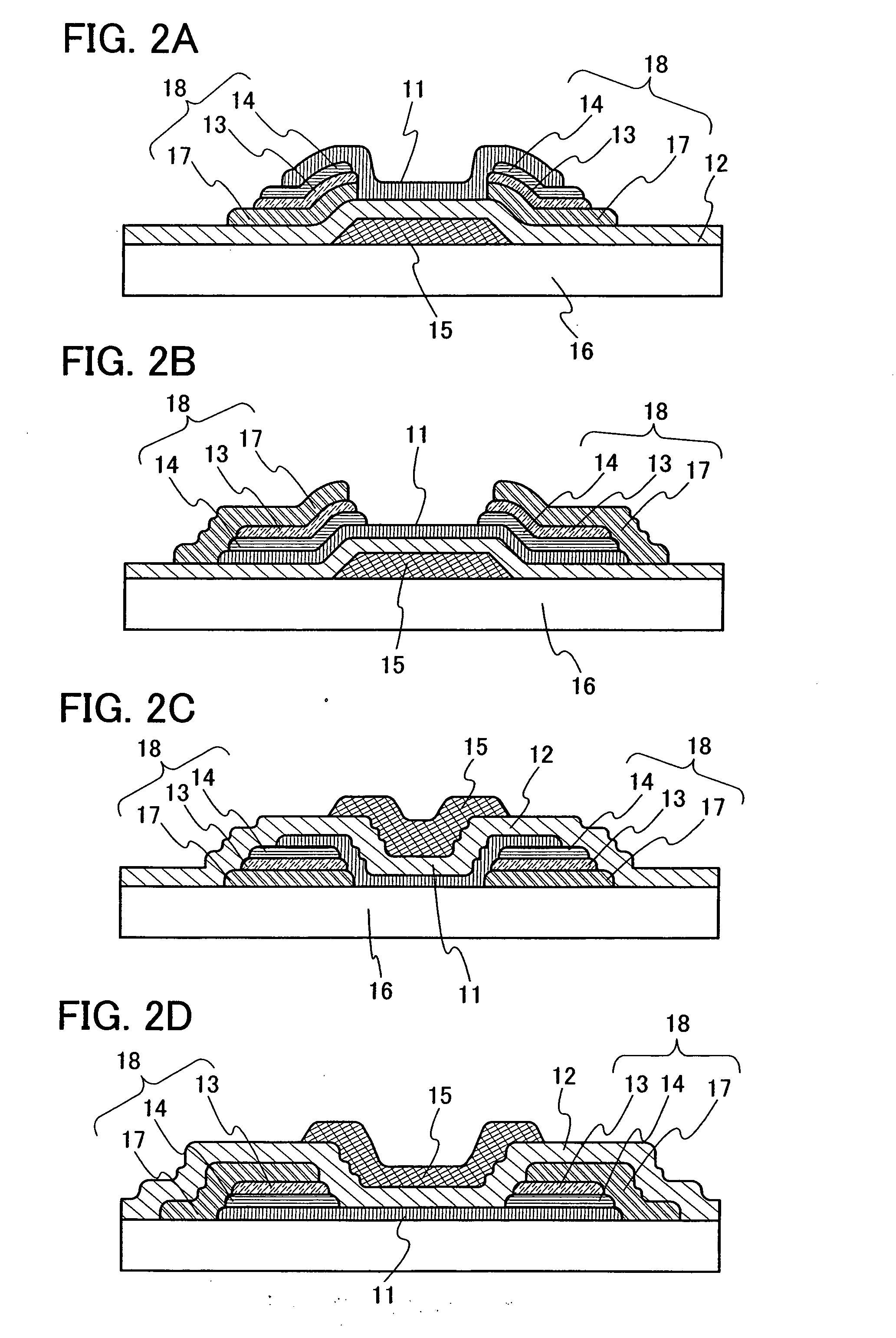
[0165]Subsequently, an example of a structure which is suitable for an n-channel organic field effect transistor and in which an electron is a carrier will be explained. This structure further includes a second layer 14 containing alkali metal, alkaline earth metal, or a compound containing alkali metal or alkaline earth metal (oxide, nitride, or salt) in addition to the structure of Embodiment Mode 1 including the composite layer 13 in part of the source electrode or the drain electrode.
[0166]An organic semiconductor material used in the present invention is not particularly limited. However, in particular, as an organic semiconductor material having characteristics as an n-channel field effect transistor, the following material is preferable: perylene tetra carboxylic anhydride and a derivative thereof, a perylene tetra carboxylic diimide derivative, naphthalene tetra carboxylic anhydride and a derivative thereof, a naphthalene tetra carboxylic diimide derivative, a metallophthalo...
embodiment mode 3
[0178]Subsequently, a structure in which an organic compound used for a composite layer is also used for a semiconductor layer will be explained. In this structure, the same organic compound is used for the composite layer and the semiconductor layer; thus, the manufacturing process is simplified and is advantageous in terms of the cost. Further, since adhesion between the semiconductor layer and a source and drain electrode, and chemical stability at the interface are improved, further improvement in transistor characteristics can be expected. In addition, improvement in durability of an organic filed effect transistor can be expected.
[0179]A semiconductor material used in the present invention is not particularly limited; however, in this embodiment mode, since the same organic compound as that used for the composite layer is used, the carbazole derivative represented by the above general formula (1) is preferable.
[0180]The structure of FIG. 1A is used as an example in order to ex...
PUM
 Abstract
Description
Claims
Application Information
 - R&D
- Intellectual Property
- Life Sciences
- Materials
- Tech Scout
- Unparalleled Data Quality
- Higher Quality Content
- 60% Fewer Hallucinations
Browse by: Latest US Patents, China's latest patents, Technical Efficacy Thesaurus, Application Domain, Technology Topic, Popular Technical Reports.
© 2025 PatSnap. All rights reserved.Legal|Privacy policy|Modern Slavery Act Transparency Statement|Sitemap|About US| Contact US: help@patsnap.com


