
Gate-all-around type semiconductor device and method of manufacturing the same

a technology of all-around and semiconductor devices, which is applied in the direction of semiconductor devices, electrical devices, nanotechnology, etc., can solve the problems of high gidl, high gate leakage current, and deterioration of the channel driving capability of the gate electrode, so as to reduce the leakage current and increase the distance between the gate electrode and the source/drain layer.

Active Publication Date: 2008-04-03
SAMSUNG ELECTRONICS CO LTD
View PDF14 Cites 58 Cited by
  • Summary
  • Abstract
  • Description
  • Claims
  • Application Information

AI Technical Summary

Benefits of technology

[0007]Example embodiments provide a gate-all-around (GAA) type semiconductor device, in which a gate induced drain leakage (GIDL) and / or a gate leakage current may be reduced.
[0008]Example embodiments provide a method of manufacturing a GAA type semiconductor device, in which a GIDL and / or a gate leakage current may be reduced.
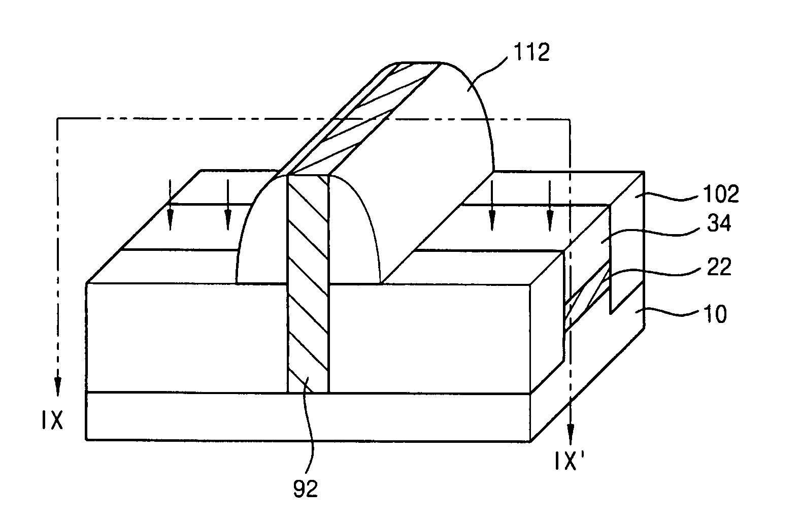
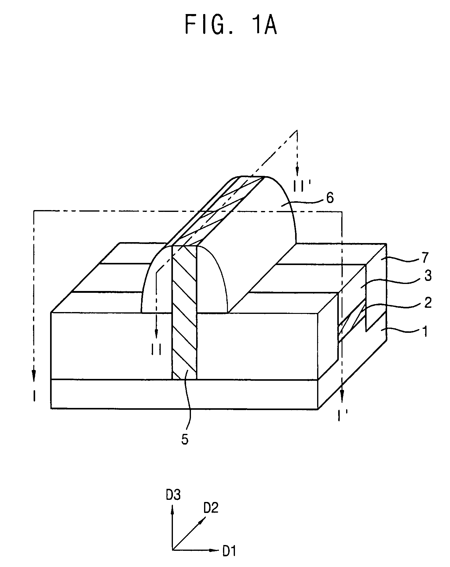
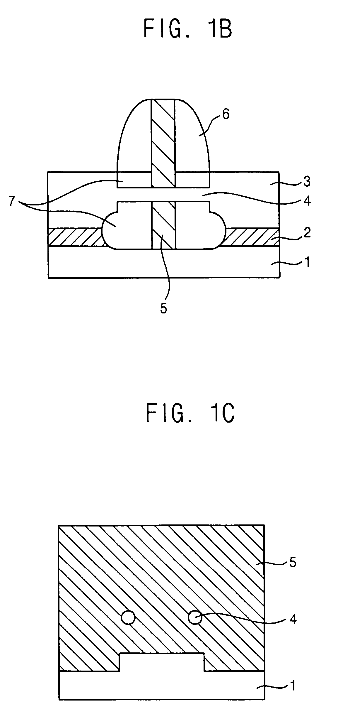
[0028]In an example embodiment, in a gate-all-around (GAA) type semiconductor device having a nanowire channel, a size of a gate electrode may be reduced and an insulation layer pattern may be formed between the gate electrode and a source / drain layer. Thus, an area at which the gate electrode makes contact with the source / drain layer may be reduced so that a gate induced drain leakage (GIDL) may be reduced. Additionally, a gate leakage current may be reduced because a distance between the gate electrode and the source / drain layer may be increased. Furthermore, the gate electrode may have a size smaller than that of a conventional gate electrode so that the GAA type semiconductor device may be advantageous with respect to physical space requirements, and general integration.

Problems solved by technology

If the channel length of the MOS transistor is reduced, a short channel effect, e.g., an effect of a source / drain region on an electric field of a channel region, may be increased and a channel driving capability of a gate electrode may be deteriorated.
However, as the gate electrode makes contact with the source / drain region at a broad area, solving the above problems of the high GIDL and the high gate leakage current may not be easy.

Method used


Image

  • Gate-all-around type semiconductor device and method of manufacturing the same
  • Gate-all-around type semiconductor device and method of manufacturing the same
  • Gate-all-around type semiconductor device and method of manufacturing the same

Examples


Embodiment Construction

[0035]Example embodiments having thus been described, it will be obvious that the same may be varied in many ways. Such variations are not to be regarded as a departure from the intended spirit and scope of example embodiments, and all such modifications as would be obvious to one skilled in the art are intended to be included within the scope of the following claims.

[0036]Detailed example embodiments are disclosed herein. However, specific structural and functional details disclosed herein are merely representative for purposes of describing example embodiments. Example embodiments may, however, be embodied in many alternate forms and should not be construed as limited to only the embodiments set forth herein.

[0037]Accordingly, while example embodiments are capable of various modifications and alternative forms, embodiments thereof are shown by way of example in the drawings and will herein be described in detail. It should be understood, however, that there is no intent to limit e...


PUM


Abstract

The gate-all-around (GAA) type semiconductor device may include source / drain layers, a nanowire channel, a gate electrode and an insulation layer pattern. The source / drain layers may be disposed at a distance in a first direction on a semiconductor substrate. The nanowire channel may connect the source / drain layers. The gate electrode may extend in a second direction substantially perpendicular to the first direction. The gate electrode may have a height in a third direction substantially perpendicular to the first and second directions and may partially surround the nanowire channel. The insulation layer pattern may be formed between and around the source / drain layers on the semiconductor substrate and may cover the nanowire channel and a portion of the gate electrode. Thus, a size of the gate electrode may be reduced, and / or a gate induced drain leakage (GIDL) and / or a gate leakage current may be reduced.

Description

PRIORITY STATEMENT[0001]This application claims priority under 35 U.S.C. §119 to Korean Patent Application No. 2006-97082, filed on Oct. 2, 2006, in the Korean Patent Office, the entire contents of which are incorporated herein by reference.BACKGROUND[0002]1. Field[0003]Example embodiments relate to a semiconductor device and a method of manufacturing the same. More particularly, example embodiments relate to a gate-all-around (GAA) type semiconductor device and a method of manufacturing the same.[0004]2. Description of Related Art[0005]As an integration degree of semiconductor devices has increased, a size of a region for forming unit cells, e.g., a size of an active region has been reduced, and thus a channel length of a metal-oxide-semiconductor (MOS) transistor formed in the active region has been reduced. If the channel length of the MOS transistor is reduced, a short channel effect, e.g., an effect of a source / drain region on an electric field of a channel region, may be incre...

Claims


Application Information

Patent Timeline
IPC IPC(8): H01L29/78H01L21/336
CPCB82Y10/00H01L29/0665H01L29/78696H01L29/42392H01L29/0673
Inventor SUK, SUNG-DAEKIM, DONG-WONYEO, KYOUNG-HWAN
Owner SAMSUNG ELECTRONICS CO LTD
Learn More