
Semiconductor device with a field stop zone and process of producing the same

a technology of semiconductor devices and stop zones, which is applied in the direction of semiconductor devices, semiconductor/solid-state device details, electrical equipment, etc., can solve the problems of affecting the switching and breakdown voltage characteristics of devices

Active Publication Date: 2008-03-06
INFINEON TECH AUSTRIA AG
View PDF3 Cites 124 Cited by
  • Summary
  • Abstract
  • Description
  • Claims
  • Application Information

AI Technical Summary

Problems solved by technology

In particular, thickness and concentration of the field stop zone greatly affect the switching and breakdown voltage characteristics of the device.

Method used


Image

  • Semiconductor device with a field stop zone and process of producing the same
  • Semiconductor device with a field stop zone and process of producing the same
  • Semiconductor device with a field stop zone and process of producing the same

Examples


Embodiment Construction

[0012]The following detailed description refers to the accompanying drawings that show, by way of illustration, specific details and embodiments in which the invention may be practiced. These embodiments are described in sufficient detail to enable those skilled in the art to practice the invention. Other embodiments may be utilized and structural, logical, and electrical changes may be made without departing from the scope of the invention. The various embodiments are not necessarily mutually exclusive, as some embodiments can be combined with one or more other embodiments to form new embodiments.

[0013]In the following description, the terms “wafer” and “substrate” may be used interchangeably to refer generally to any structure on which integrated circuits are formed and also to such structures during various stages of integrated circuit fabrication. The term “substrate” is understood to include a semiconductor wafer. The term “substrate” is also used to refer to semiconductor stru...


PUM


Abstract

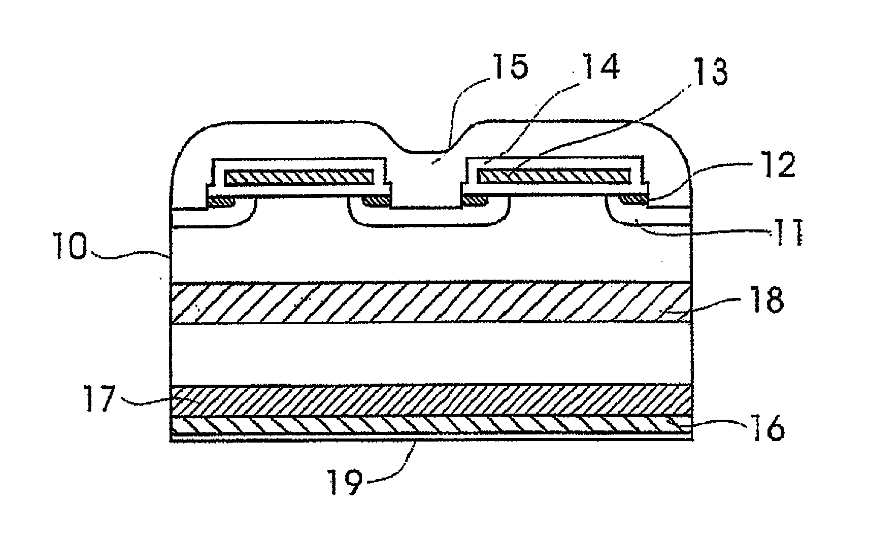
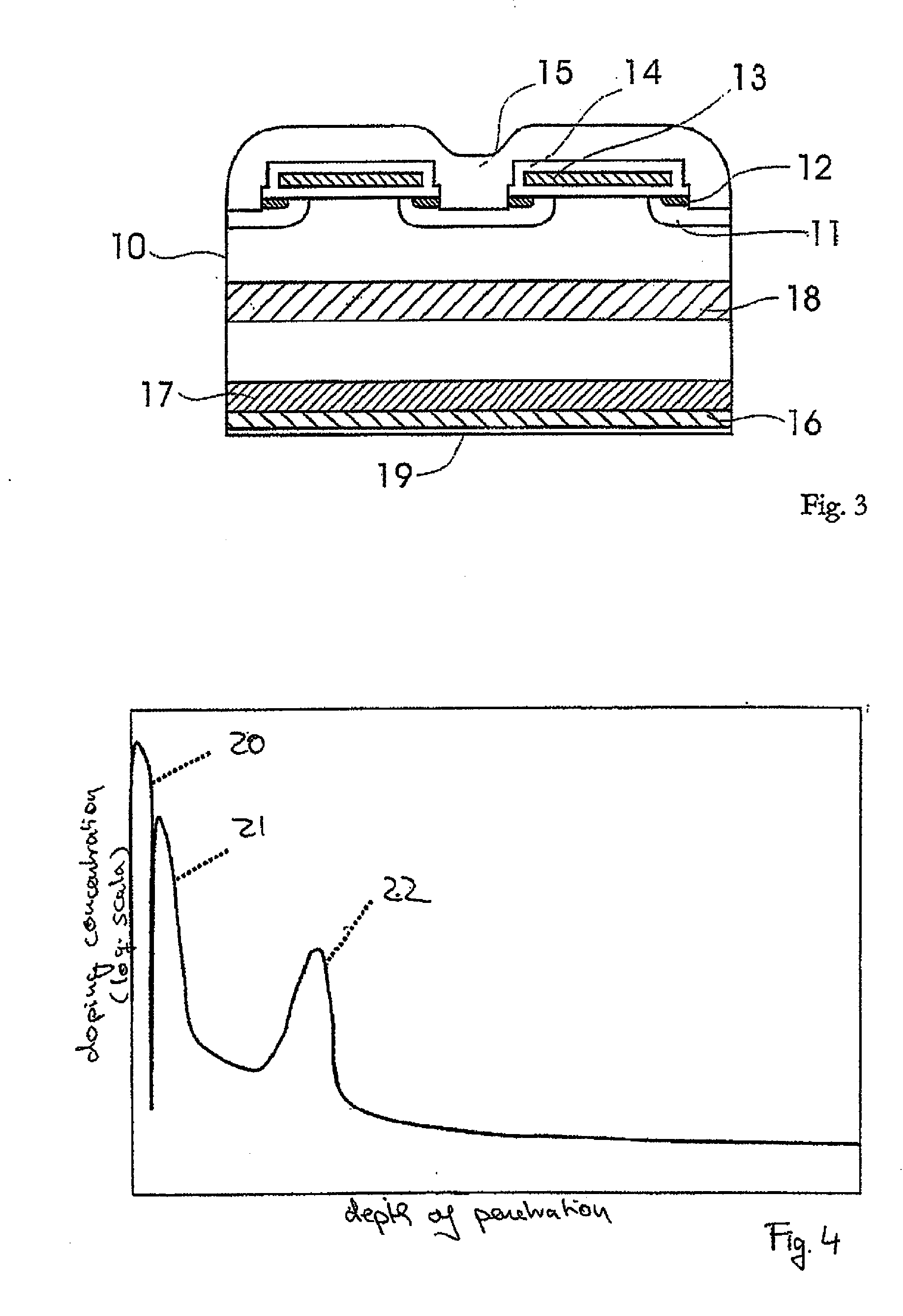
Embodiments discussed herein relate to processes of producing a field stop zone within a semiconductor substrate by implanting dopant atoms into the substrate to form a field stop zone between a channel region and a surface of the substrate, at least some of the dopant atoms having energy levels of at least 0.15 eV below the energy level of the conduction band edge of semiconductor substrate; and laser annealing the field stop zone.

Description

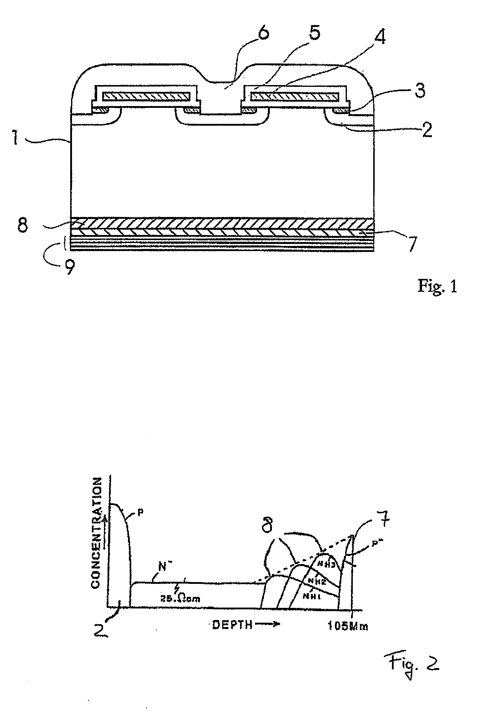
TECHNICAL FIELD[0001]The subject matter disclosed herein generally relates to the semiconductor devices and processes for making them, and more specifically, to an insulated gate bipolar transistors, IGBTs, with field stop zones.BACKGROUND INFORMATION[0002]IGBTs have been made as punch-through devices (PT-IGBT) in which a DMOS type structure is formed at the top of an epitaxially deposited silicon substrate. The epitaxial layer is formed atop a higher concentration buffer layer, of the same conductivity type, which is in turn formed on a substrate of opposite conductivity type and which acts as a minority carrier injection source. In such punch-through devices, the electric field across the silicon substrate under reverse bias reaches from the top surface of the silicon to the buffer layer, which also acts as a depletion layer stop.[0003]Field stop IGBTs, on the other hand, are made starting from a low doped substrate of a first conductivity type without employing epitaxial layers. ...

Claims


Application Information

Patent Timeline
IPC IPC(8): H01L29/739H01L21/8249
CPCH01L29/0834H01L29/167H01L29/7395H01L29/36H01L29/32
Inventor SCHULZE, HANS-JOACHIMPFIRSCH, FRANKVOSS, STEPHANNIEDERNOSTHEIDE, FRANZ-JOSEF
Owner INFINEON TECH AUSTRIA AG
Learn More