
Display system with single crystal Si thin film transistors

a thin film transistor and display system technology, applied in the field of single crystal si thin film transistors, can solve the problems of limiting the use of large-size lcd panels, low current density, poor transistor performance of amorphous silicon tfts, etc., and achieves the reduction of current leakage of tfts, the effect of high display contrast ratio and reduced single crystal si of tfts

Active Publication Date: 2008-02-28
KOPIN CORPORATION
View PDF12 Cites 9 Cited by
  • Summary
  • Abstract
  • Description
  • Claims
  • Application Information

AI Technical Summary

Benefits of technology

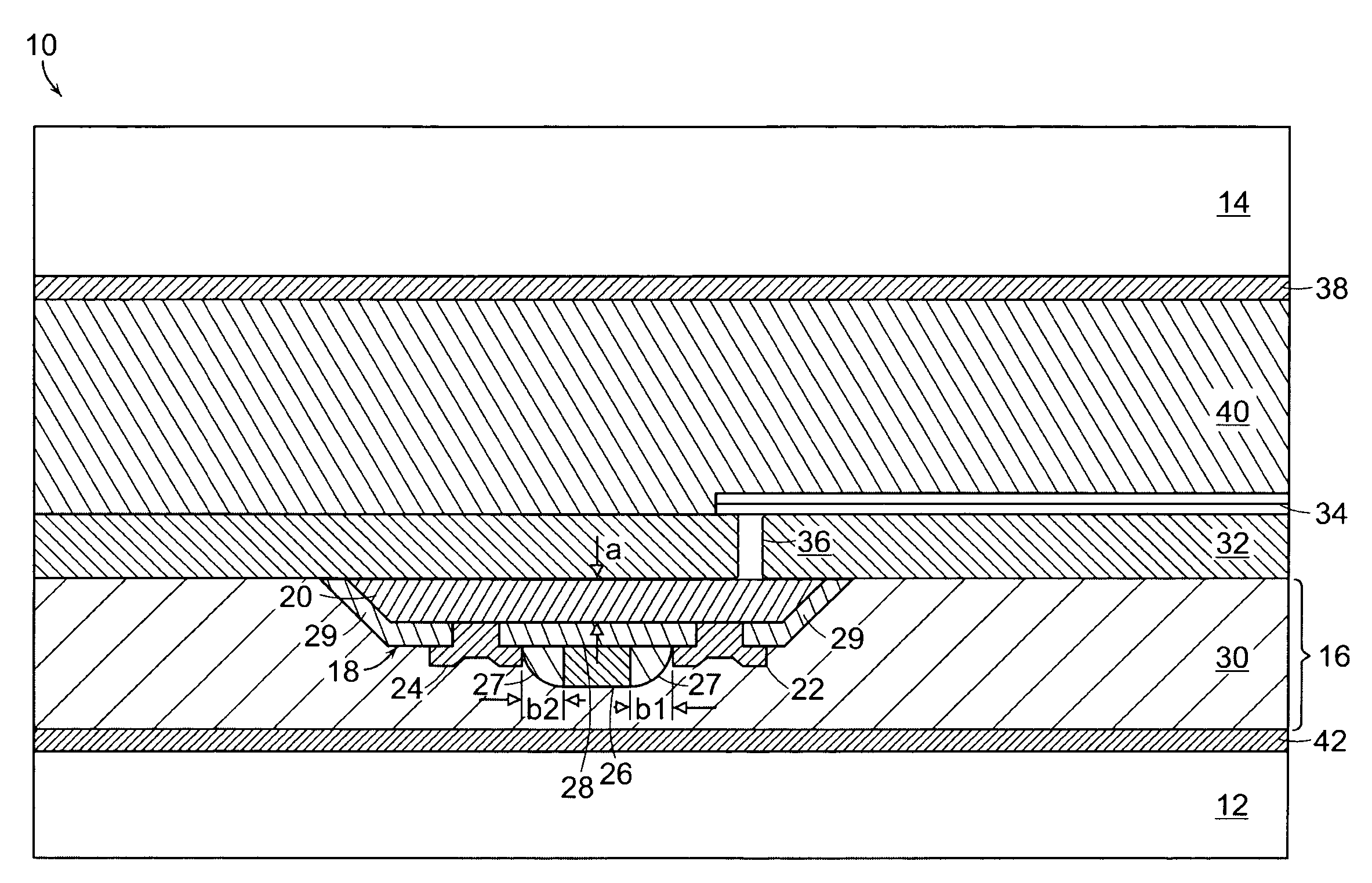
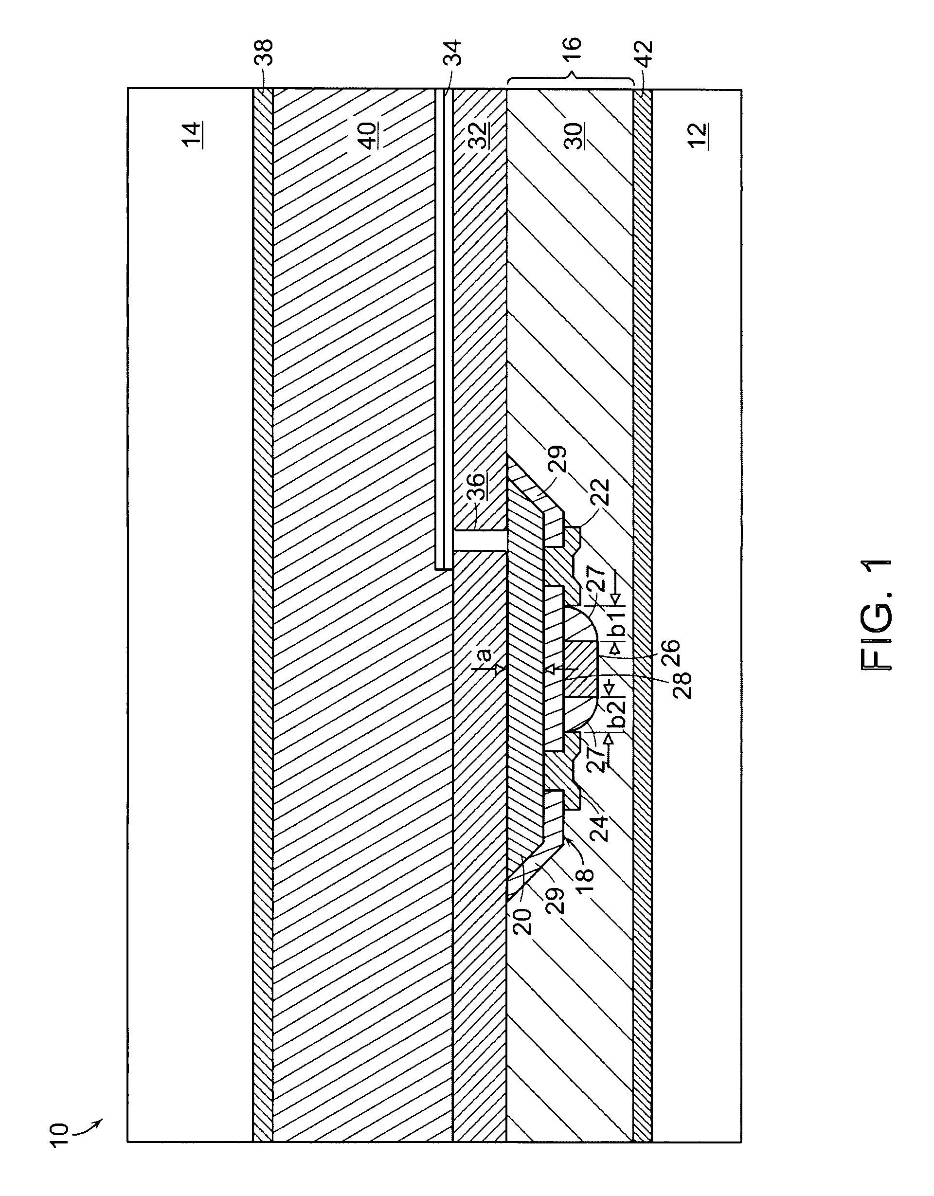
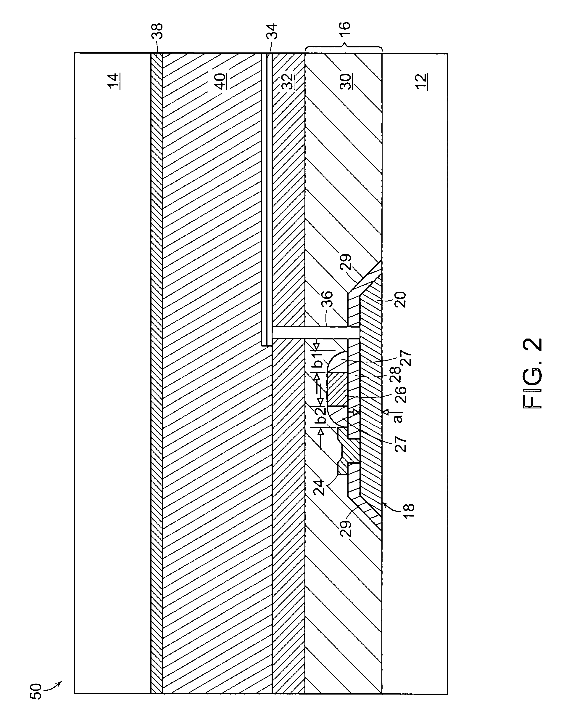
[0009] An LCD of the invention, employing an array of pixel TFTs, each of which includes a thin film layer of essentially single crystal Si that has a thickness in a range of between about 100 nm and about 200 nm, can provide a high display contrast ratio. In particular, this thickness of the Si thin film layer is relatively very thin compared with a typical thickness of about 300 nm or greater of conventional transistors employed in LCDs in the art. With such relatively thin TFTs, photosensitivity of single crystal Si of the TFTs (backlighting and / or ambient light photosensitivity) can be substantially reduced, which results in reduction of current leakage of the TFTs. This reduction of current leakage of the TFTs can provide a relatively high display contrast ratio, even when LCDs, in which they are incorporated, are being used in ambient (or external) light environment, or when backlighting is very bright.
[0010] Also, an LCD of the present invention, employing TFTs of essentially single crystal Si, can provide better performance, such as higher pixel density and faster frequency response, than LCDs employing amorphous Si TFTs or polycrystalline TFTs.

Problems solved by technology

Amorphous silicon TFTs generally have poor transistor performance because of very low electron mobility of amorphous silicon.
As a result, the amorphous silicon TFTs can only deliver low current density, limiting their use to large-size LCD panels that can accommodate large-size TFTs.
In addition, single crystal TFTs have high frequency response, allowing the control electronic circuits to be monolithically integrated within the display panel.
With such thickness, the pixel TFTs may have relatively high photosensitivity (e.g., backlighting and / or ambient light photosensitivity), which can result in current leakage of pixel TFTs.
Such current leakage of pixel TFTs, in turn, can cause a relatively low display contrast ratio and / or high image retention.

Method used


Image

  • Display system with single crystal Si thin film transistors
  • Display system with single crystal Si thin film transistors
  • Display system with single crystal Si thin film transistors

Examples


example 1

PERFORMANCE DATA OF LCDS OF THE INVENTION

[0058] A standard LCD as a control, and an LCD of the invention, each of which was a QVGA resolution display, were tested for their performance. The standard LCD included TFTs having the thickness of about 300-320 nm and the LCD of the invention included TFTs having the thickness of between about 150-200 nm. The pixel electrode material is polycrystalline Si. As shown in Table 1, the LCD of the invention had superior properties, for example, in image retention, photosensitivity, brightness and contrast ratio.

TABLE 1LCD of theStandard LCDInventionUnitsContrast Ratio90115White / BlackTransmission2.5%2.5%White / BacklightMax Display350700cd / m2BrightnessMax Backlight14,00028,000cd / m2BrightnessMax Ambient Light2001000LuxPhotosensitivity(diffused)Flicker (60 Hz)−40−60dBImage Retention  1%0.5%% of full gray scale


PUM

PropertyMeasurementUnit
thicknessaaaaaaaaaa
thicknessaaaaaaaaaa
thicknessaaaaaaaaaa

Abstract

A liquid crystal display comprises a display panel that includes at least one pixel transistor, at least one pixel electrode in electrical communication with the pixel transistor, at least one common electrode, and a liquid crystal material between the pixel electrode and the common electrode. The pixel transistor includes a thin film layer of essentially single crystal silicon that has a thickness in a range of between about 100 nm and about 200 nm. The pixel electrode has a thickness in a range of between about 5 nm and about 20 nm. The common electrode has a thickness of between about 50 nm and about 200 nm.

Description

RELATED APPLICATION [0001] This application claims the benefit of U.S. Provisional Application No. 60 / 838,014, filed on Aug. 16, 2006, the entire teachings of which are incorporated herein by reference.BACKGROUND [0002] Active matrix color liquid crystal displays (LCDs) generally include five different components: a white light source, a first polarizing film that is mounted on one side of a display panel including an array of pixels defined by arrays of pixel electrodes and thin-film pixel transistors (TFTs), a color filter plate containing at least three primary colors arranged into pixels covered with a transparent common electrode and finally a second polarizing film. A liquid crystal material is disposed between the pixel and common electrodes. This material will rotate the polarization of light when an electric field is applied across it. Thus, when a particular pixel of the display is turned on, the liquid crystal material rotates polarized light transmitted through the mater...

Claims


Application Information

Patent Timeline
Patent Type & Authority Applications(United States)
IPC IPC(8): G02F1/136
CPCG02F1/1362H01L29/78654H01L27/1266H01L27/1214G02F1/13439
Inventor TSAUR, BOR-YEUCHOI, HONGLO, JASON
Owner KOPIN CORPORATION
Learn More