
Plasma display panel and related technologies

a technology of display panel and plasma, which is applied in the manufacture of discharge tube luminescnet screens, electric discharge tubes/lamps, electrode systems, etc., can solve the problems of metallic element short circuit, the electrodes of the upper panel are at risk of being exposed, and the upper dielectric layer formed at the upper panel may be damaged

Inactive Publication Date: 2008-01-31
LG ELECTRONICS INC
View PDF8 Cites 22 Cited by
  • Summary
  • Abstract
  • Description
  • Claims
  • Application Information

AI Technical Summary

Benefits of technology

[0014] The discharge delay time of the plasma display panel may be 1.2 microseconds or less. The surface discharge start voltage of the...

Problems solved by technology

However, during the occurrence of an electric discharge in the plasma display panel, the upper dielectric layer formed at the upper panel may be damaged due to a shock caused by positive ions.
Therefore, the electrodes of the upper panel have a risk of being exposed and short-circuited by a metallic element such as sodium, etc.

Method used


Image

  • Plasma display panel and related technologies
  • Plasma display panel and related technologies
  • Plasma display panel and related technologies

Examples


Embodiment Construction

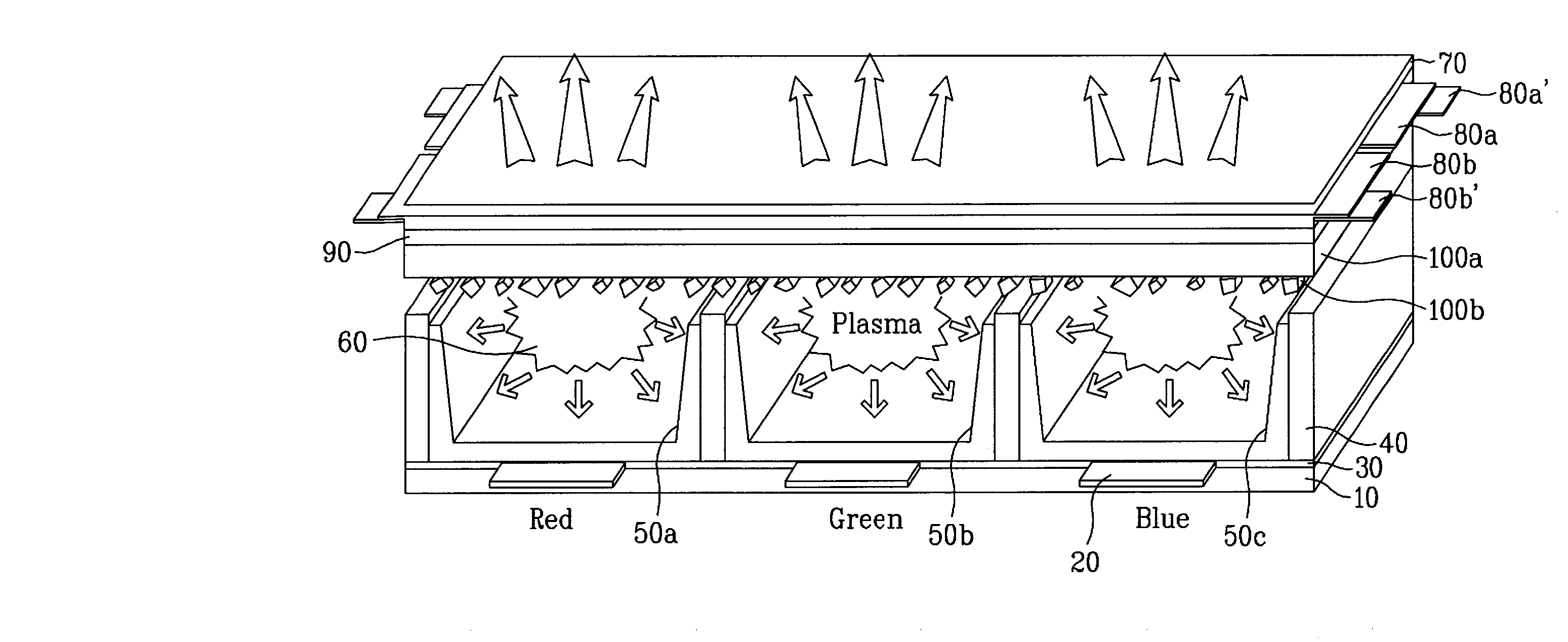
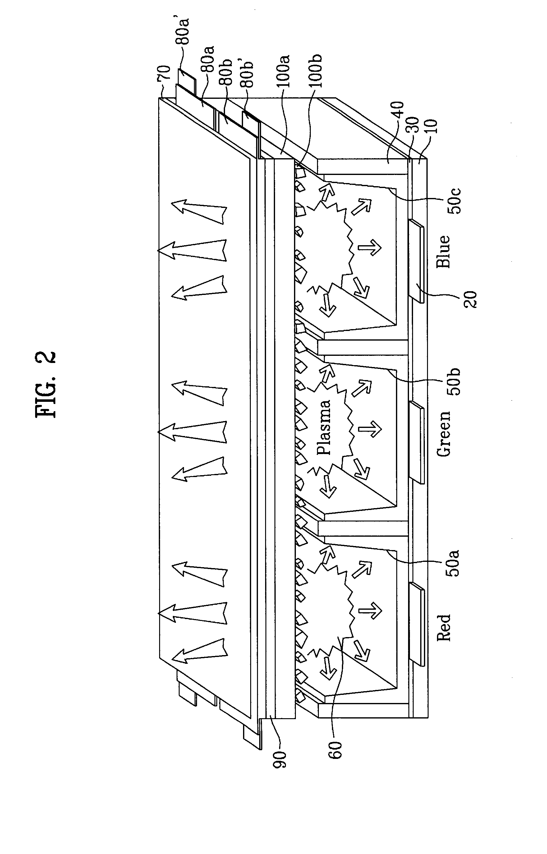
[0030] A plasma display panel may have a first protective film and a second protective film formed on the first protective film. The second protective film may contain a metallic oxide having a maximum cathode ray luminescence value within a wavelength region of 300 to 500 nanometers. Such a second protective film may improve jitter characteristics and discharge efficiency of the plasma display panel.

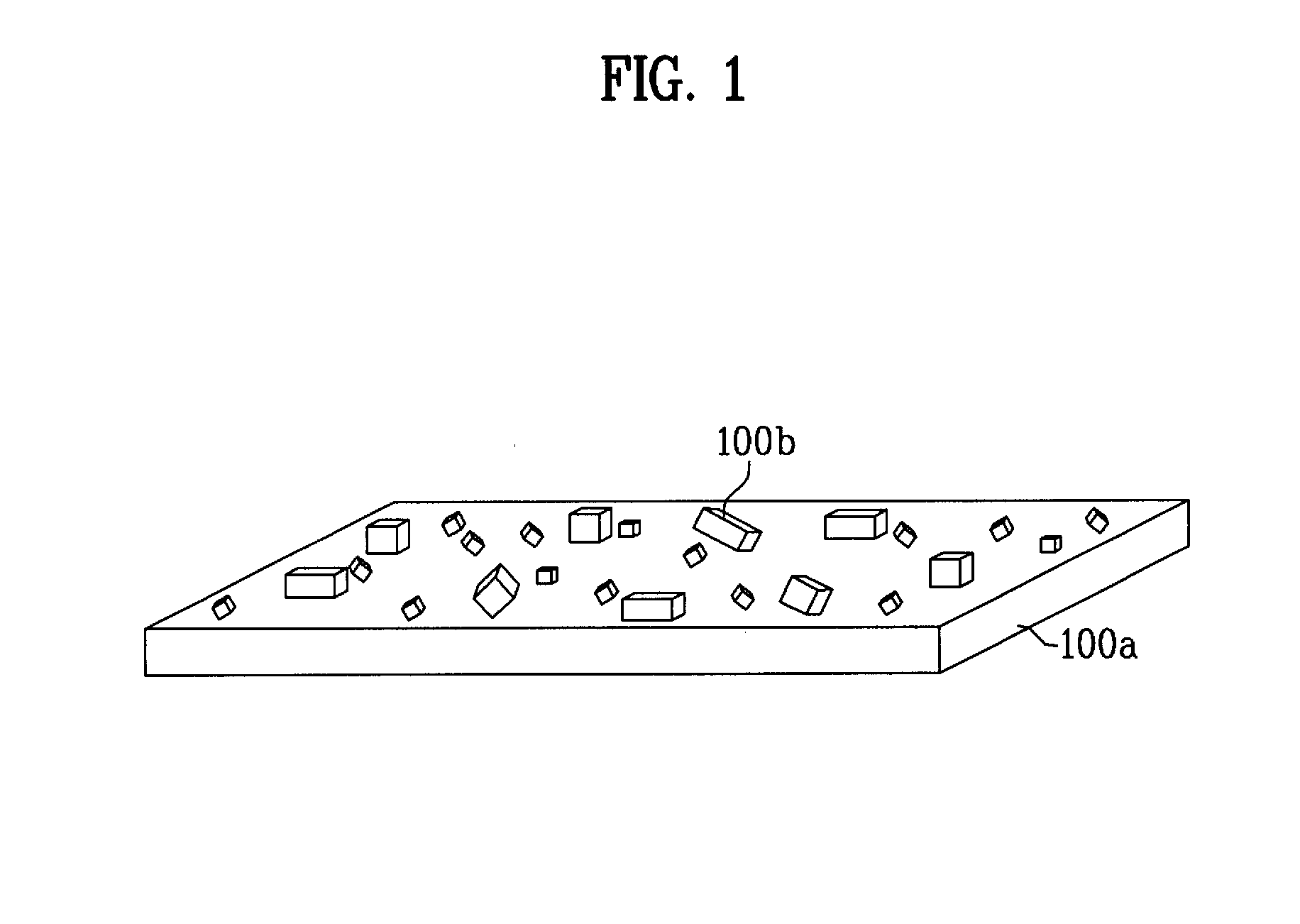
[0031] The metallic oxide of the second protective layer may be distributed on the first protective layer in the form of lumps. Such distribution may form an uneven surface. Thus, during a gas discharge in the plasma display panel, ultraviolet ions collide with the protective layer in an increase surface area, which increases the discharge amount of secondary electrons and lowers a discharge start voltage. This further improves jitter characteristics and discharge efficiency of the plasma display panel.

[0032]FIG. 1 is a view illustrating an example configuration of protective layers i...


PUM


Abstract

A protective layer of a plasma display panel is disclosed. In the plasma display panel including a first panel and a second panel arranged to face each other while interposing barrier ribs therebetween, the plasma display panel further includes a first protective layer formed on a dielectric layer of the first panel, and a second protective layer formed on the first protective layer and containing a metallic oxide having a maximum cathode ray luminescence value within a wavelength region of 300 to 500 nanometers.

Description

[0001] This application claims the benefit of the Korean Patent Application No. 10-2006-0071601, filed on Jul. 28, 2006, Korean Patent Application No. 10-2006-0071600, filed on Jul. 28, 2006, Korean Patent Application No. 10-2007-0008805, filed on Jan. 29, 2007, which are hereby incorporated by reference in their entireties. BACKGROUND [0002] 1. Technical Field [0003] This document relates to a display apparatus with a protective layer and related technologies. [0004] 2. Discussion of the Related Art [0005] With the advent of the multimedia age, there is demand for larger display apparatus capable of representing colors close to natural colors. To this end, a liquid crystal display (LCD), plasma display panel (PDP), projection television (TV), etc. are becoming popular rapidly in the field of a large-size high definition image. [0006] A plasma display panel includes a lower panel having address electrodes, an upper panel having sustain electrode pairs, and discharge cells defined by...

Claims


Application Information

Patent Timeline
IPC IPC(8): H01J1/62C01B13/14H01J9/02H01J11/22H01J11/24H01J11/34H01J11/40
CPCH01J9/02H01J11/40H01J11/12
Inventor KIM, BO HYUNPARK, MIN SOOPARK, DEOK HAIRYU, BYUNG GILKIM, YOUNG SUNGSONG, MOON BONGCHO, WON KI
Owner LG ELECTRONICS INC
Learn More