Image display device

Inactive Publication Date: 2008-01-31
HITACHI DISPLAYS
View PDF2 Cites 2 Cited by
  • Summary
  • Abstract
  • Description
  • Claims
  • Application Information

AI Technical Summary

Benefits of technology

[0016] The frame body having such a particular shape as described in patent document 1 may have the possibility of bringing about drawbacks such as the difficulty in taking a material for forming the frame body per se, the increase of a weight of the liquid crystal display device along with the large-sizing of the liquid crystal display device, the expansion of sizes of both substrates. Further, when the frame widths of all sizes of the frame body are uniformly narrowed to overcome the drawbacks which the patent document 1 possesses, there arises the possibility of occurrence of leaking of vacuum. The leaking of vacuum brings about the deterioration of a degree of vacuum in a vacuum display region thus giving rise to a drawback the reliability of the image display device is damaged. Further, when the possibility of occurrence of leaking of vacuum can be eliminated, the narrower a width of the sealing region, the possibility of occurrence attributed to flowing of the sealing material is decreased and hence, the narrowing of the width of the sealing region is desirable.
[0017] Accordingly, it is an object of the present invention to provide a highly reliable and prolonged-lifetime image display device which can realize the miniaturization and the reduction of weight and can eliminate the occurrence of leaking of vacuum in a sealing region.
[0022] By fixing the frame width of each side of the frame body, there arises no waste in taking a material for the frame body and the frame body can be manufactured at a low cost thus contributing to the large-sizing of products in the years to come. Further, by adopting the frame widths corresponding to lengths of the respective sides, profiles of substrates can be made small thus contributing to the miniaturization of a profile of a product and the reduction of weight of the product. Still further, along with the enhancement of substrate design, the occurrence of leaking of vacuum can be prevented thus realizing the acquisition of the reliable and prolonged-lifetime image display device.
[0023] Further, it is possible to suppress the flowing of a sealing material to an undesired portion by controlling a quantity of the sealing material to be used thus enhancing the operability and ensuring the display quality.

Problems solved by technology

The frame body having such a particular shape as described in patent document 1 may have the possibility of bringing about drawbacks such as the difficulty in taking a material for forming the frame body per se, the increase of a weight of the liquid crystal display device along with the large-sizing of the liquid crystal display device, the expansion of sizes of both substrates.
Further, when the frame widths of all sizes of the frame body are uniformly narrowed to overcome the drawbacks which the patent document 1 possesses, there arises the possibility of occurrence of leaking of vacuum.
The leaking of vacuum brings about the deterioration of a degree of vacuum in a vacuum display region thus giving rise to a drawback the reliability of the image display device is damaged.

Method used


Image

  • Image display device
  • Image display device
  • Image display device

Examples


embodiment 1

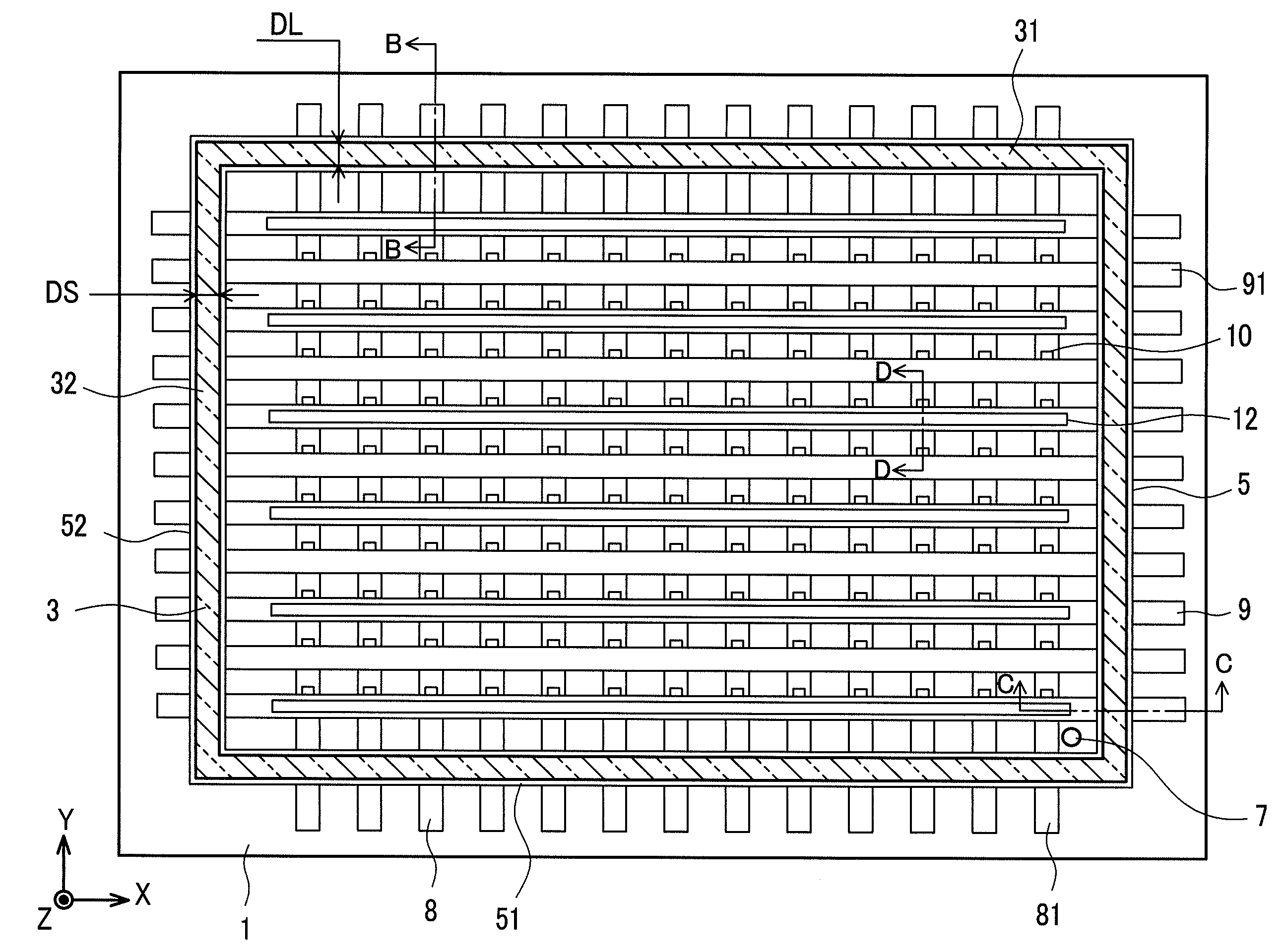
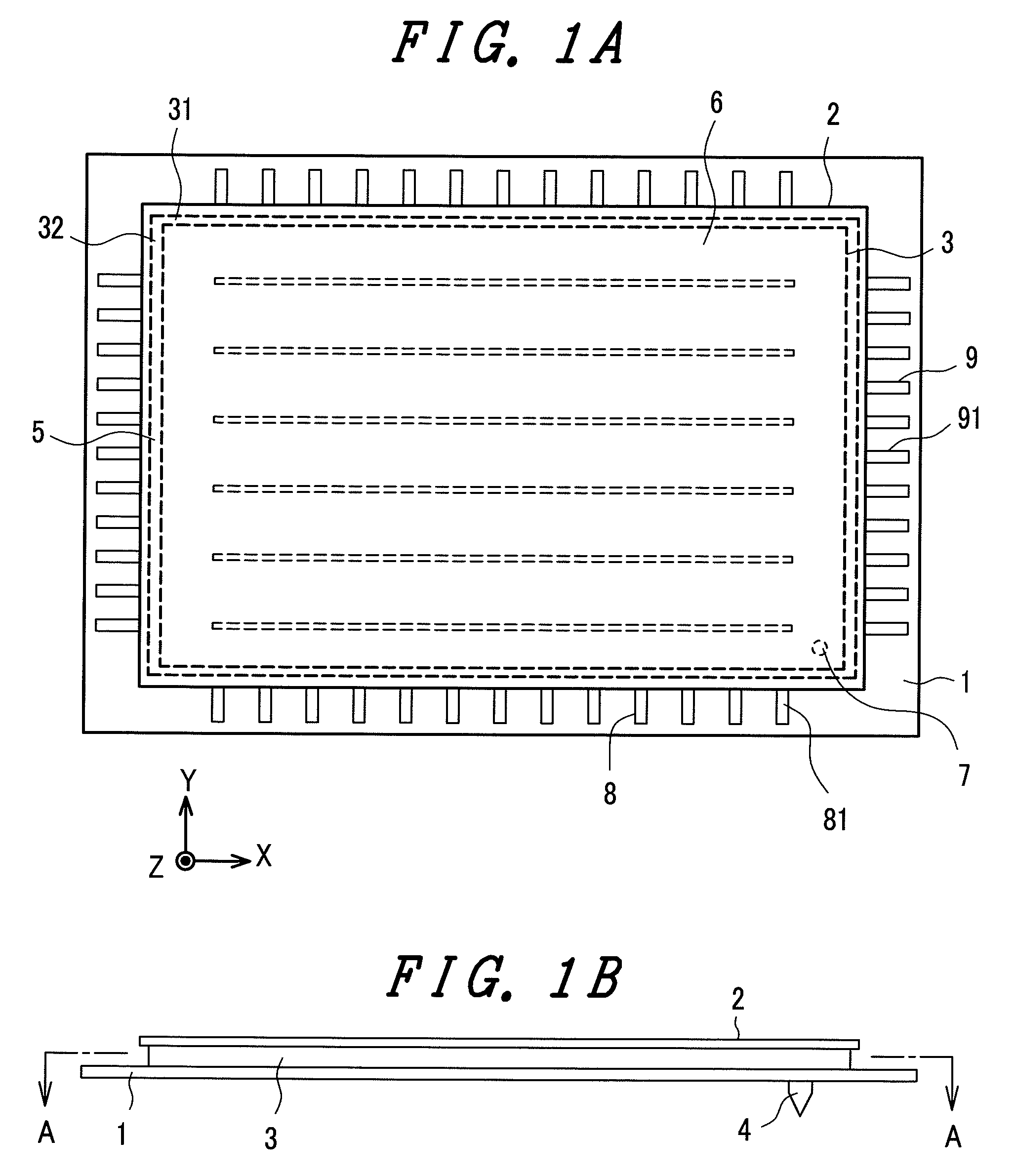
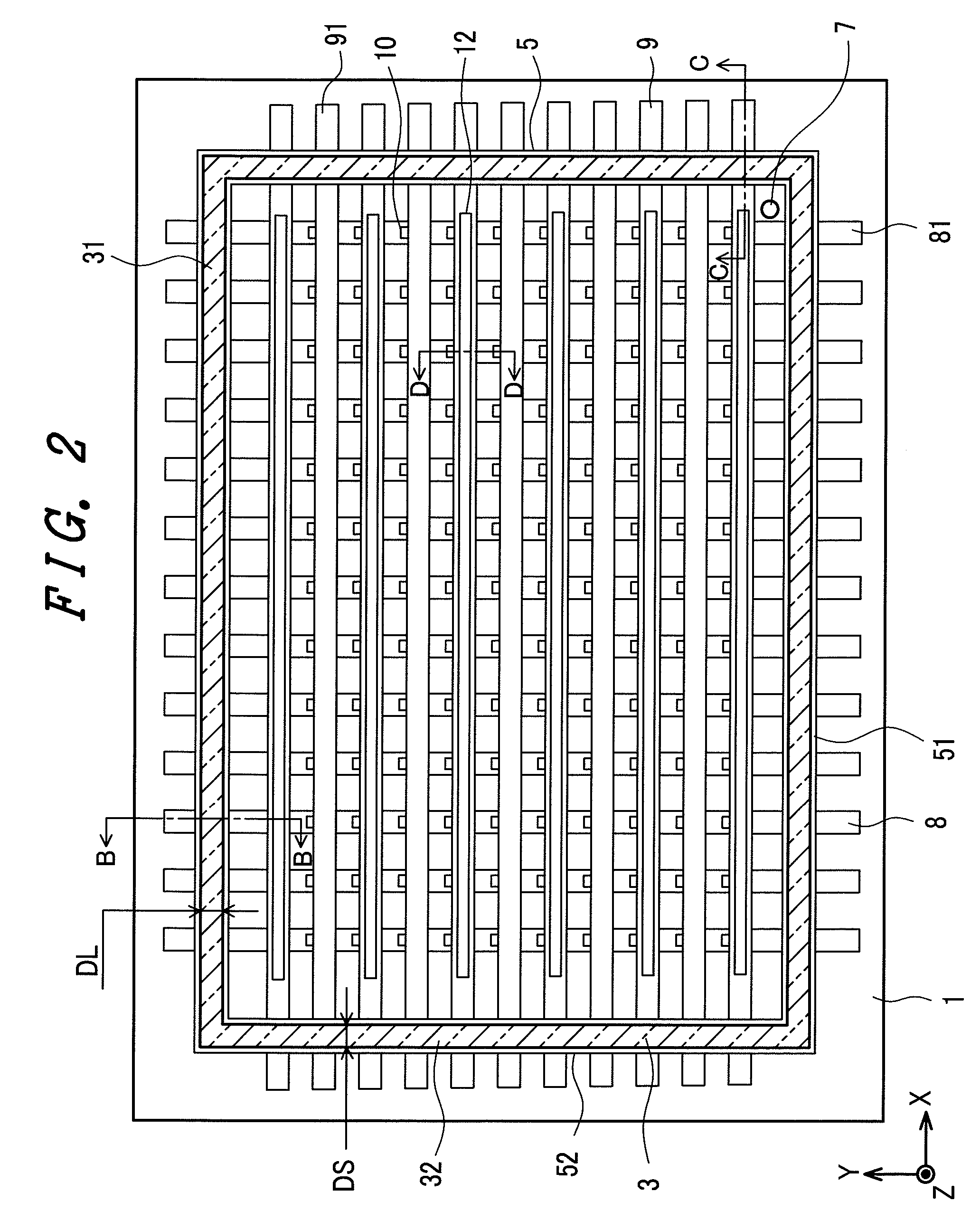
[0031]FIG. 1 to FIG. 5 are views for explaining one embodiment of an image display device according to the present invention. FIG. 1A is a plan view as viewed from a face substrate side, FIG. 1B is a side view of the image display device shown in FIG. 1A, FIG. 2 is a schematic plan view taken along a line A-A in FIG. 1B, FIG. 3 is a schematic cross-sectional view of the back substrate taken along a line B-B in FIG. 2 and a schematic cross-sectional view of the face substrate at a portion corresponding to the back substrate, FIG. 4 is a schematic cross-sectional view of the back substrate taken along a line C-C in FIG. 2 and a schematic cross-sectional view of the face substrate at a portion corresponding to the back substrate, and FIG. 5 is a schematic cross-sectional view of the back substrate taken along a line D-D in FIG. 2 and a schematic cross-sectional view of the face substrate at a portion corresponding to the back substrate.

[0032] In FIG. 1 to FIG. 5, numeral 1 indicates t...


PUM


Abstract

An image display device includes a vacuum envelope which is constituted of a rectangular back substrate which arranges electron sources in the vicinity of intersecting portions of image signal electrodes and scanning signal electrodes, a rectangular face substrate which includes phosphor layers and anodes, and a frame body which is connected to peripheral regions of the respective substrates. A frame width size of a frame body is set such that the long-side frame width is larger than the short-side frame width thus realizing the miniaturization and the reduction of weight of the image display device.

Description

BACKGROUND OF THE INVENTION [0001] 1. Field of the Invention [0002] The present invention relates to a planar image display device which makes use of emission of electrons into vacuum formed between a face substrate and a back substrate. [0003] 2. Description of the Related Art [0004] As one self-luminous-type flat panel display (FPD) having electron sources which are arranged in a matrix array, an electric field emission type image display device (FED: Field Emission Display) which uses minute integrative cold cathodes and an electron emission type image display device have been known. [0005] As the cold cathode, there have been known an electron source such as a Spindt-type electron source, a surface-conducive-type electron source, a carbon-nanotube-type electron source, an MIM (Metal-Insulator-Metal) type electron source which is formed by stacking a metal layer, an insulator and a metal layer in this order, an MIS (Metal-Insulator-Semiconductor) type electron source which is for...

Claims


Application Information

Patent Timeline
IPC IPC(8): H01J63/04
CPCH01J29/862H01J2329/862H01J31/123
Inventor TACHIHARA, HIROYUKIHATORI, AKIRAOROKU, NORIYUKI
Owner HITACHI DISPLAYS
Why Eureka
Try Eureka