Waveguide-type optical device
a waveguide and optical device technology, applied in the field of waveguide-type optical devices, can solve problems such as ln modulators, and achieve the effects of reducing the drive voltage required to obtain the desired electro-optic effect, reducing the length required, and improving modulation efficiency
- Summary
- Abstract
- Description
- Claims
- Application Information
AI Technical Summary
Benefits of technology
Problems solved by technology
Method used
Image
Examples
first embodiment
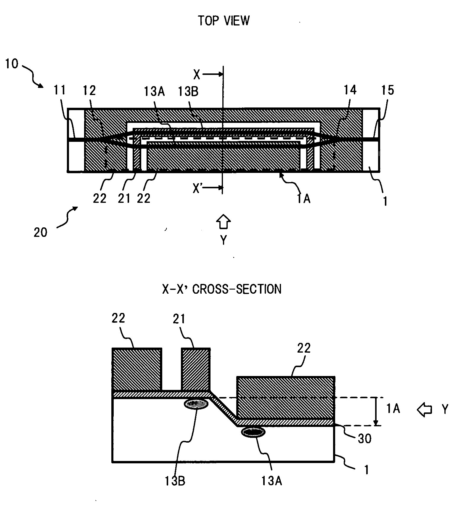
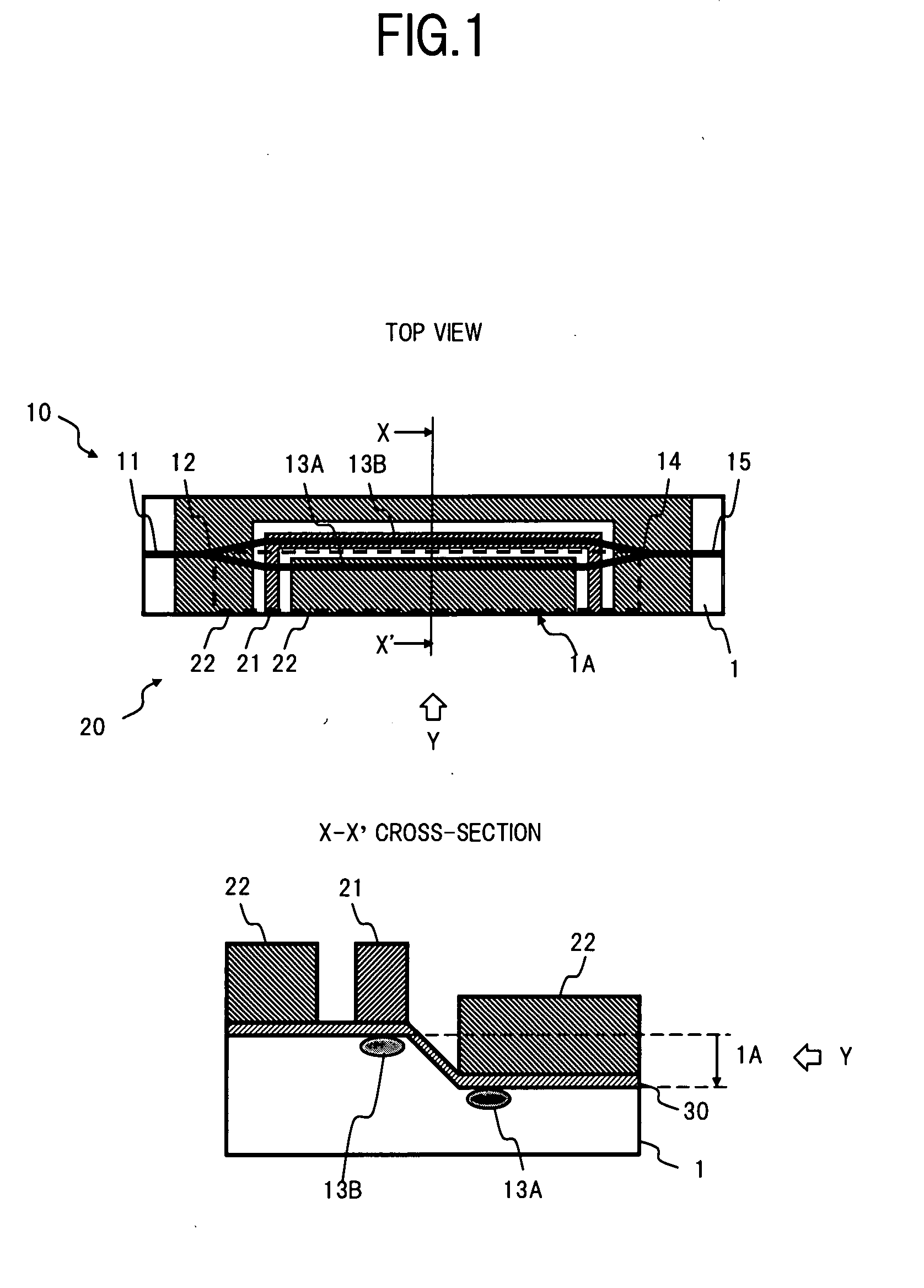
[0038]FIG. 1 is a block diagram of a waveguide-type optical device according to the present invention.
[0039]In FIG. 1, the waveguide-type optical device according to the first embodiment, is one where the present invention is applied to an LN modulator having a single-drive type electrode structure using the conventional Z-cut substrate. The LN modulator comprises: a Mach-Zehnder optical waveguide 10 including a Z-cut LN substrate 1, an input waveguide 11, a branching part 12, branching waveguides 13A and 13B, a coupling part 14, and an output waveguide 15; a drive electrode 20 including a signal electrode 21 and a ground electrode 22; and a buffer layer 30 formed between the surface of the LN substrate 1 and the drive electrode 20.
[0040]The LN substrate 1 has an etching part 1A in which the height of one face (surface) of the substrate is made different from the height of other parts, in a preset portion positioned near the branching waveguide 13A of the optical waveguide 10 (a ran...
second embodiment
[0062]Next is a description of the present invention.
[0063]FIG. 10 is block diagram showing a second embodiment of a waveguide-type optical device according to the present invention.
[0064]In FIG. 10, the waveguide-type optical device of this embodiment, as an application example of the LN modulator of the abovementioned first embodiment, is one where the fluctuations in the power of the propagation light in the branching waveguides 13A and 12B are more effectively suppressed by providing the step structure and reducing the drive voltage. More specifically, the height of the surface of the LN substrate 1 is made three stages, and with respect to the height of the input waveguide 11 and the output waveguide 15 (refer to the cross-section X1-X1′ at the center part of FIG. 10), the height of the branching waveguide 13A is made one stage lower, and the height of the branching waveguide 13B is made one stage higher (refer to the cross-section X2-X2′ at the lower part of FIG. 10).
[0065]In ...
third embodiment
[0068]Next is a description of the present invention.
[0069]FIG. 12 is a block diagram showing a third embodiment of a waveguide-type optical device according to the present invention.
[0070]In FIG. 12, the waveguide device of this embodiment, as a modified example of the LN modulator of the abovementioned first embodiment, is one where the function of the input waveguide 11 and the branching part 12, and the coupling part 14 and the output waveguide 15 formed in the LN substrate 1, is realized using optical fiber type couplers 41 and 41′ to thereby simplify the configuration of the waveguide substrate.
[0071]More specifically, regarding the LN substrate 1′ used in this LN modulator, an etching part 1E is formed on a part of an approximate half on the lower side surrounded by the broken line in the figure. The boundary portion of the etching part 1E, similarly to the case of the aforementioned first embodiment, is formed with an incline in order to prevent cutting of the branching wave...
PUM
| Property | Measurement | Unit |
|---|---|---|
| distance | aaaaa | aaaaa |
| distance | aaaaa | aaaaa |
| electric field | aaaaa | aaaaa |
Abstract
Description
Claims
Application Information
 - R&D
- Intellectual Property
- Life Sciences
- Materials
- Tech Scout
- Unparalleled Data Quality
- Higher Quality Content
- 60% Fewer Hallucinations
Browse by: Latest US Patents, China's latest patents, Technical Efficacy Thesaurus, Application Domain, Technology Topic, Popular Technical Reports.
© 2025 PatSnap. All rights reserved.Legal|Privacy policy|Modern Slavery Act Transparency Statement|Sitemap|About US| Contact US: help@patsnap.com


