
Producing SOI structure using ion shower

a technology of soi and ion shower, which is applied in the direction of basic electric elements, electrical apparatus, semiconductor devices, etc., can solve the problems of difficult replacement of silicon wafers with glass or glass-ceramic or ceramic of the type, quartz itself is a relatively expensive material, and the cost of such structures has been the cost of silicon wafers, etc., to achieve low or no surface etching, high efficiency, and large area simultaneous ion implantation

Inactive Publication Date: 2007-12-06
CORNING INC
View PDF17 Cites 88 Cited by
  • Summary
  • Abstract
  • Description
  • Claims
  • Application Information

AI Technical Summary

Benefits of technology

[0046]The present invention has the advantages of being capable of large area simultaneous ion implantation, low or no surface etch, high efficiency and low cost. Compared with beam line ion implantation, the present invention results in thinner exfoliation film with smoother surface, which reduces down-streaming thinning and polishing needs. Therefore, the present invention enables expedient, efficient and effective ion implantation that is suitable for the production of various SOI structures, including but not limited to SiOI structures, particularly SOG structures, including but not limited to SiOG structures.

Problems solved by technology

To date, a major part of the cost of such structures ha been the cost of the silicon wafer which supports the oxide layer, topped by the Si thin film, i.e., a major part of the cost has been the support substrate.
Although the use of quartz as support substrate has been mentioned in various patents (see U.S. Pat. Nos. 6,140,209, 6,211,041, 6,309,950, 6,323,108, 6335,231 and 6,391,740), quartz is itself a relatively expensive material.
In particular, it is difficult to replace a silicon wafer with a glass or glass-ceramic or ceramic of the type which can be manufactured in large quantities at low cost, i.e., it is difficult to make cost effective SOG and SiOG structures.
Another factor significantly affecting the cost of ion-implantation approach to producing SOI, SiOI, SOG and SiOG structures is the efficiency of the ion-implantation process.
However, those traditional ion-implantation processes require the use of narrow ion beams, which lead to long implantation time and high cost.
However, PIII suffers from the drawbacks of surface charging and etching by the plasma and lack of flexibility at higher energy, lack of accurate dosage control, and inability to precisely control the thickness of the ion implantation zone and the thickness of the exfoliation film.

Method used


Image

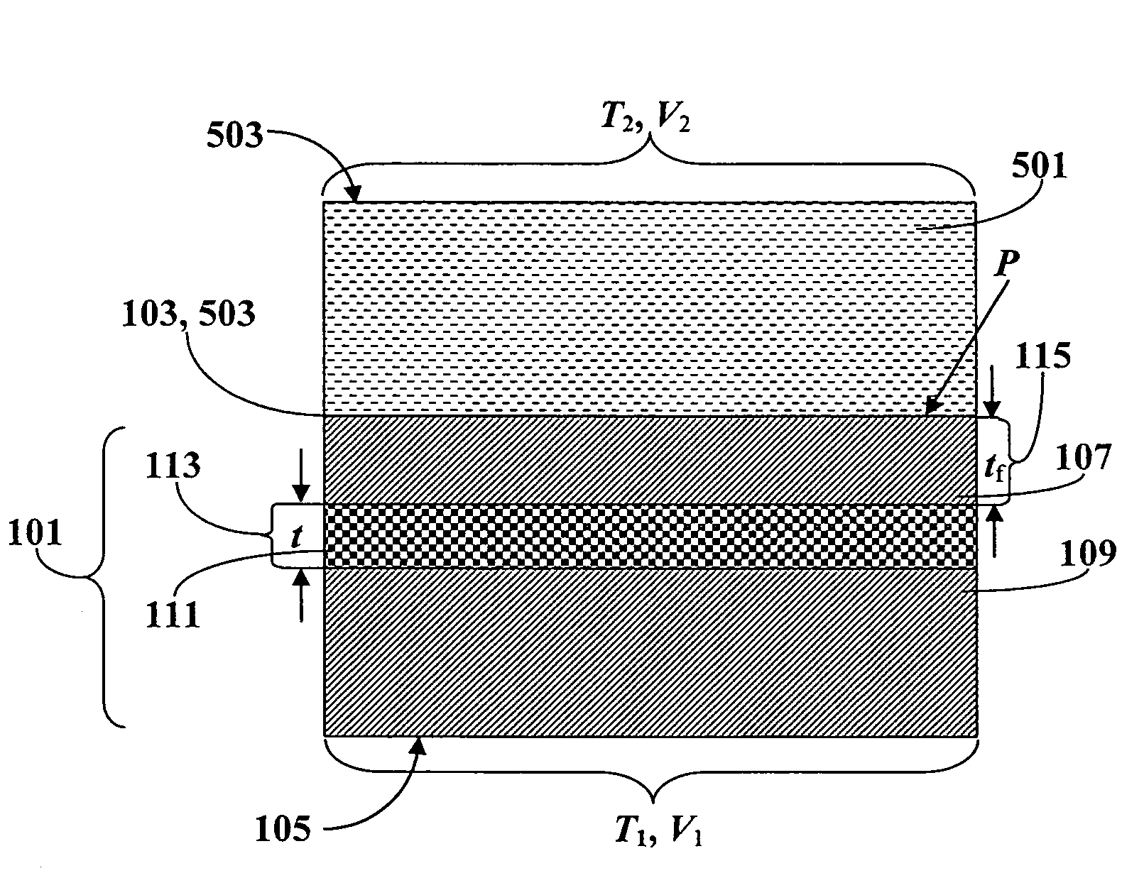
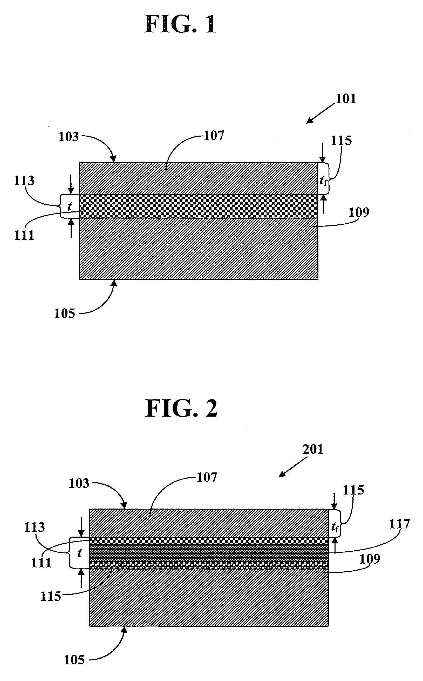
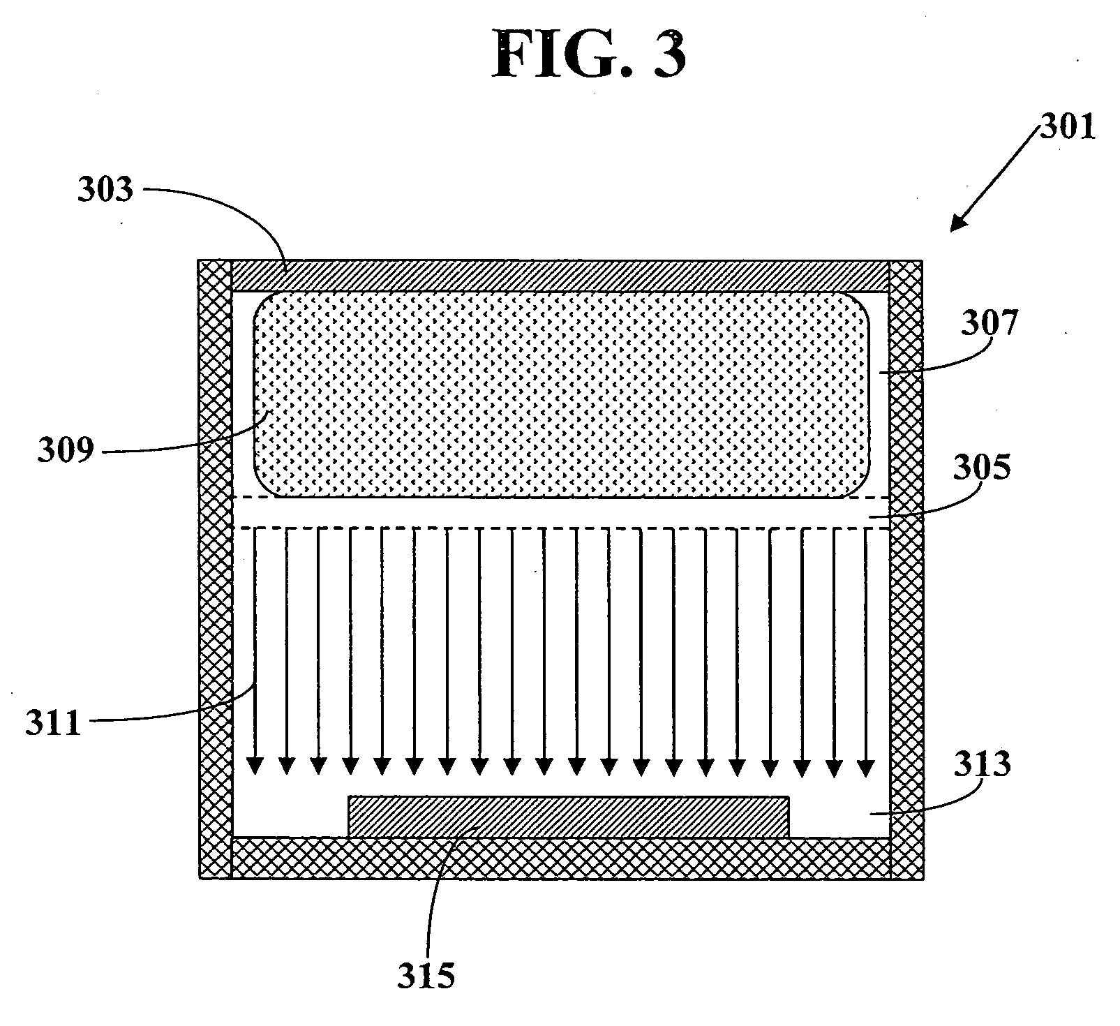
  • Producing SOI structure using ion shower
  • Producing SOI structure using ion shower
  • Producing SOI structure using ion shower

Examples


example 1

[0230]A silicon wafer 150 mm diameter, 500 microns thick was H3+ ion implanted at dosage of 2E16 (i.e., 2×10⁶) H3+ ions / cm2 and implantation energy of 50 KeV in a standard ion shower equipment. The wafer was then treated in oxygen plasma to oxidize the surface groups. An Corning Incorporated Eagle 2000™ glass wafer 100 mm in diameter was then washed with Fischer scientific Contrad 70 detergent in ultrasonic bath for 15 minutes followed by distilled water wash for 15 minutes in ultrasonic bath and then washed in 10% nitric acid followed by distilled water wash again. Both these wafers were finally cleaned in spin washer dryer with distilled water in the clean room.

[0231]The two wafers were then brought into contact ensuring that no air was trapped between the wafers and then the wafers were introduced into the bonder and bonded as taught in US 2004 / 0229444 A1. The glass wafer was placed on the negative electrode and the silicon wafer was placed on the positive electrode. The two wafe...

example 2

[0232]The experiment of Example 1 was repeated but with following changes. The silicon wafer was implanted with H3+ at an energy of 60 KeV at the same dosage. It was found that the silicon film bonded to the glass was 262 nm thick.


PUM


Abstract

Disclosed are methods for making SOI and SOG structures using ion shower for implanting ions to the donor substrate. The ion shower provides expedient, efficient, low-cost and effective ion implantation while minimizing damage to the exfoliation film.

Description

FIELD OF THE INVENTION[0001]The present invention relates to processes for making semiconductor-on-insulator (“SOI”) structures. In particular, the present invention relates to processes for making SOI structures by using ion shower implantation. The present invention is useful, for example, in the manufacture of semiconductor-on-insulator structures such as silicon-on-insulator structures, semiconductor-on-glass structures such as silicon-on-glass structures, and related semiconductor devices.BACKGROUND OF THE INVENTION[0002]As used herein, the abbreviation “SiOI” refers to silicon-on-insulator. The abbreviation “SOI” refers to semiconductor-on-insulator in general, including but not limited to SiOI. The abbreviation “SiOG” refers to silicon-on-glass. The abbreviation “SOG” refers to semiconductor-on-glass in general, including but not limited to SiOG. SOG is intended to include semiconductor-on-ceramics and semiconductor-on-glass-ceramics structures. Likewise, SiOG is intended to ...

Claims


Application Information

Patent Timeline
IPC IPC(8): H01L21/46
CPCH01L21/187H01L21/20H01L21/265H01L27/12
Inventor CITES, JEFFREY SCOTTGADKAREE, KISHOR PURUSHOTTAMMASCHMEYER, RICHARD ORR
Owner CORNING INC
Learn More