Combined design of optical and image processing elements
a technology of optical and image processing elements, applied in the field of digital imaging, can solve the problems of not meeting other requirements of camera specifications, not providing the required output image quality, etc., and achieve the effect of reducing blur in the digital output imag
- Summary
- Abstract
- Description
- Claims
- Application Information
AI Technical Summary
Benefits of technology
Problems solved by technology
Method used
Image
Examples
Embodiment Construction
Definitions
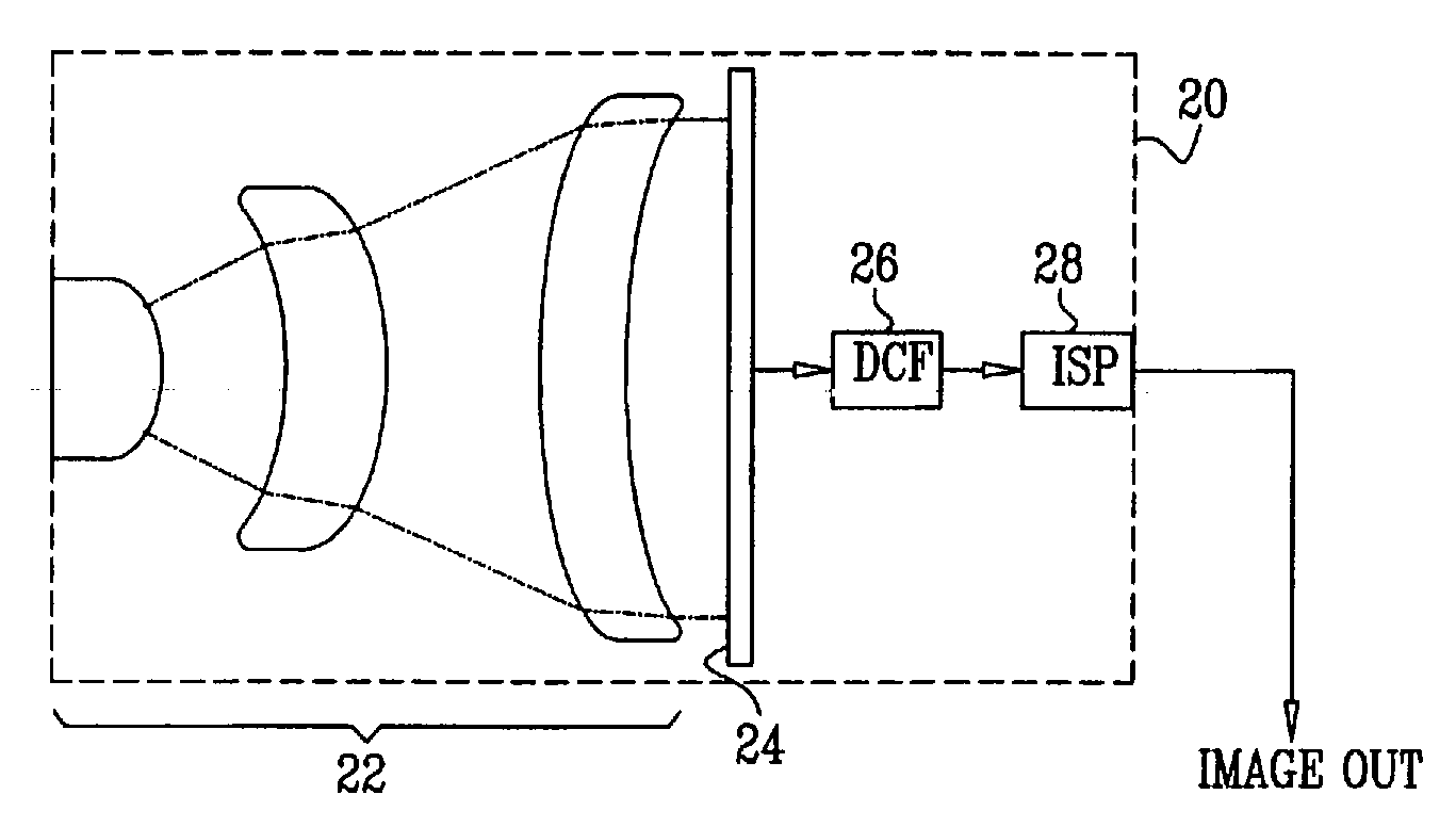
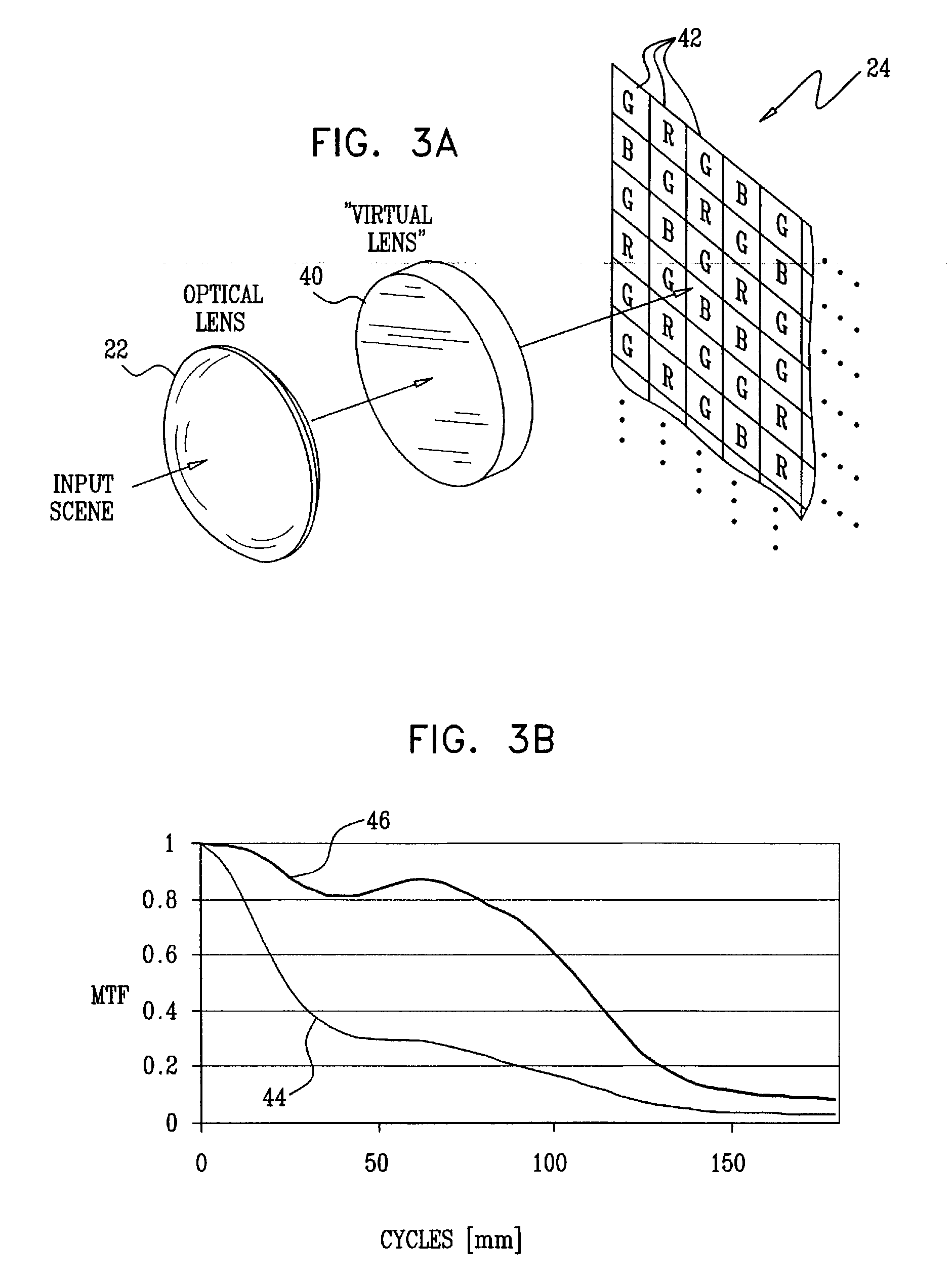
[0043] The following is a non-exhaustive list of technical terms that are used in the present patent application and in the claims. Although these terms are used herein in accordance with the plain meaning accorded the terms in the art, they are listed below for the convenience of the reader in understanding the following description and the claims. [0044] Pitch of a detector array refers to the center-to-center distance between elements of the array. [0045] Cylindrical symmetry describes a structure, such as a simple or compound lens, which has an optical axis such that the structure is invariant under rotation about the optical axis for any and all angles of rotation. [0046] Point spread function (PSF) is the impulse response of an optical system in the spatial domain, i.e., the image formed by the system of a bright point object against a dark background. [0047] Extent of the PSF is the full width at half maximum (FWHM) of the PSF. [0048] Optical transfer function (OT...
PUM
 Abstract
Description
Claims
Application Information
 - R&D
- Intellectual Property
- Life Sciences
- Materials
- Tech Scout
- Unparalleled Data Quality
- Higher Quality Content
- 60% Fewer Hallucinations
Browse by: Latest US Patents, China's latest patents, Technical Efficacy Thesaurus, Application Domain, Technology Topic, Popular Technical Reports.
© 2025 PatSnap. All rights reserved.Legal|Privacy policy|Modern Slavery Act Transparency Statement|Sitemap|About US| Contact US: help@patsnap.com


