Level shifting multiplexing circuit for connecting a two conductor full duplex bus to a bidirectional single conductor bus

Inactive Publication Date: 2007-08-09
KYOCERA CORP
View PDF9 Cites 8 Cited by
  • Summary
  • Abstract
  • Description
  • Claims
  • Application Information

AI Technical Summary

Benefits of technology

[0004] A level shifting multiplexing circuit provides an interface between a two conductor full duplex bus (two conductor bus) and a single conductor bidirectional half duplex bus (single conductor bus) where the two conductor bus operates at a first supply voltage and the single conductor bus operates at a second supply voltage. A first switching circuit connected between the single conductor bus and the reception conductor of the two conductor bus is configured to provide a low logic signal to the reception conductor when a first switching voltage threshold is exceeded and to provide a high logic signal, otherwise. A s

Problems solved by technology

Conventional designs utilizing single conductor buses, however, are limited in that the devices connected to the single conductor bus must operate at the same voltage as the devices communicating on the two conductor bus.

Method used


Image

  • Level shifting multiplexing circuit for connecting a two conductor full duplex bus to a bidirectional single conductor bus
  • Level shifting multiplexing circuit for connecting a two conductor full duplex bus to a bidirectional single conductor bus
  • Level shifting multiplexing circuit for connecting a two conductor full duplex bus to a bidirectional single conductor bus

Examples


Embodiment Construction

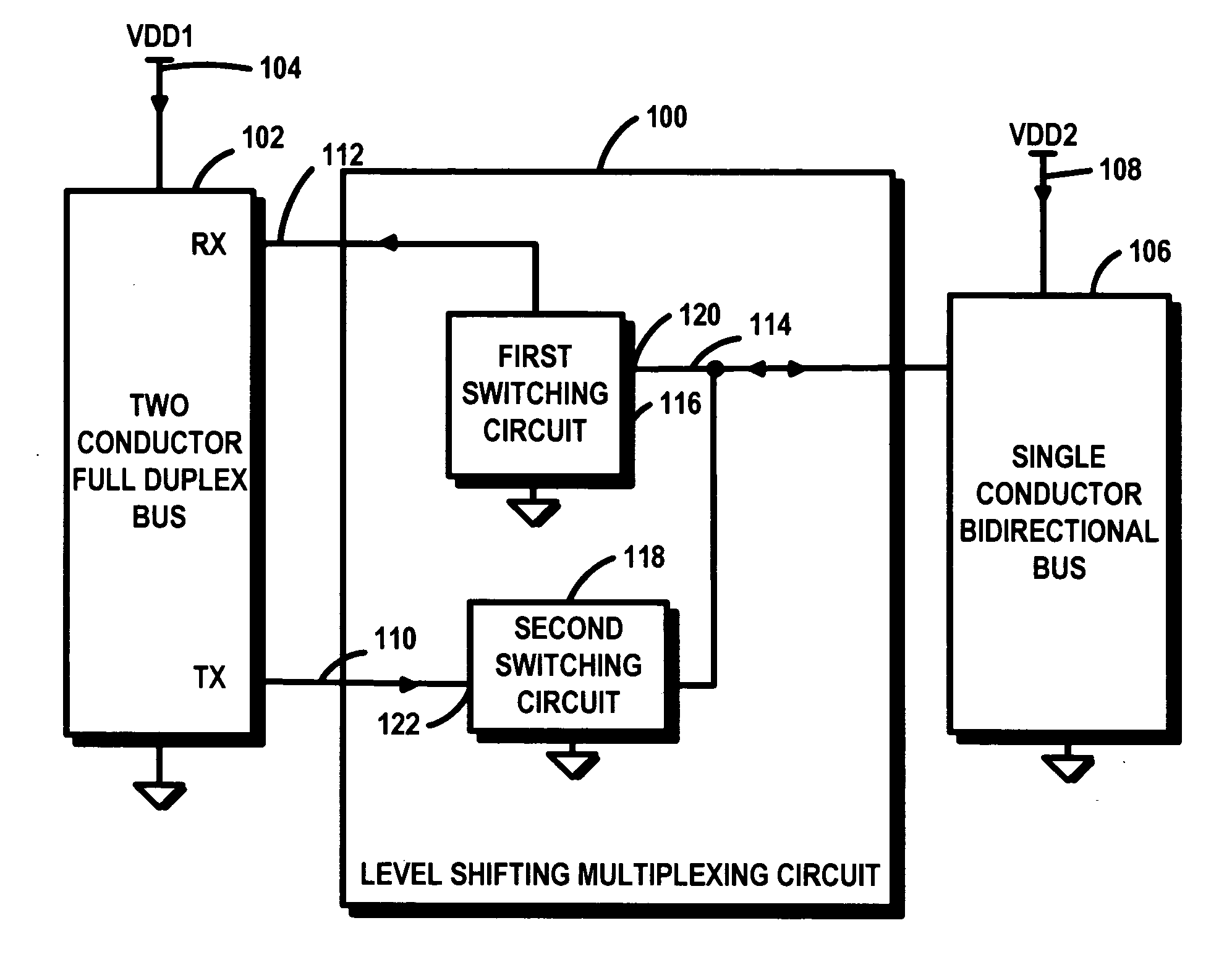
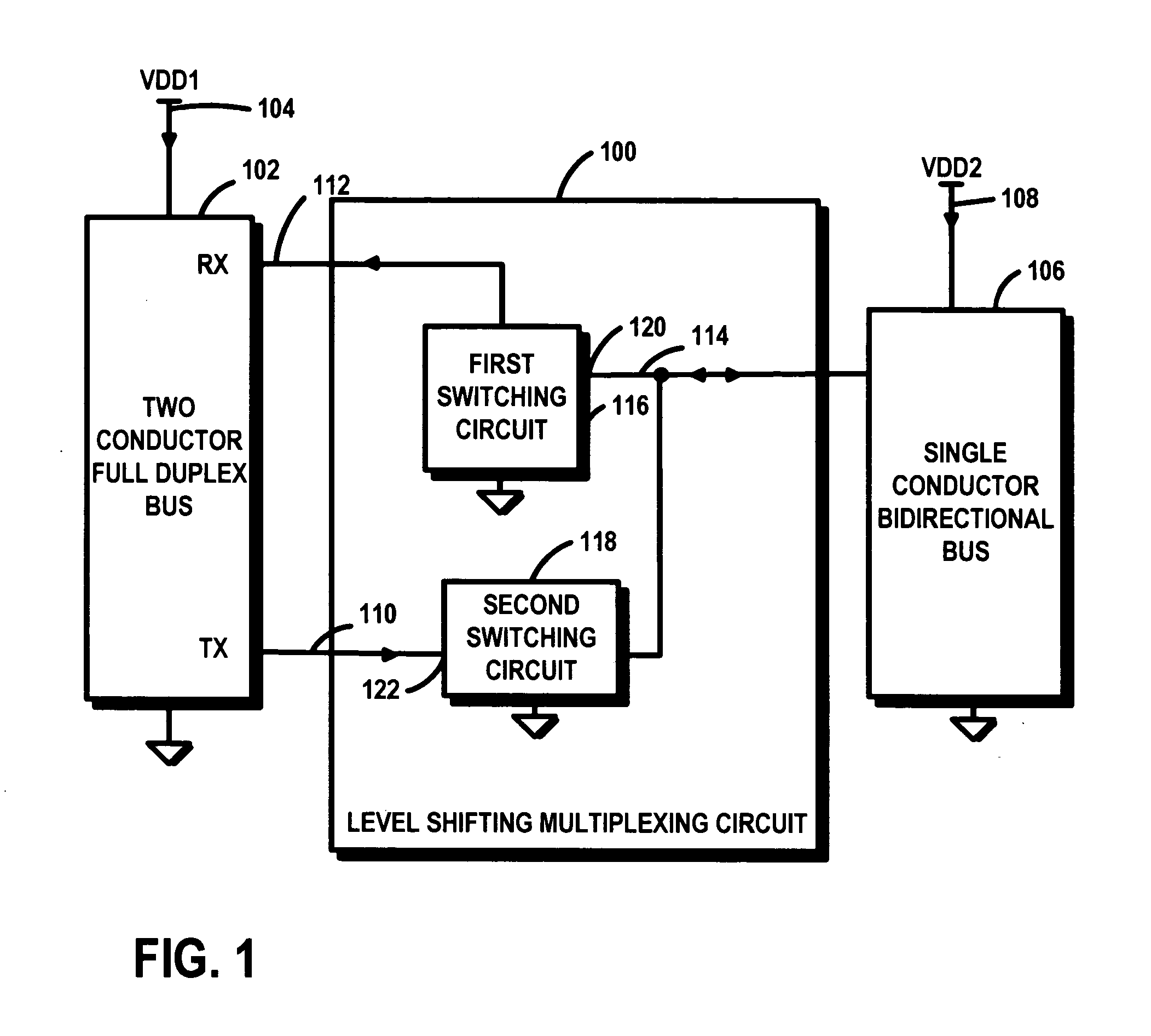
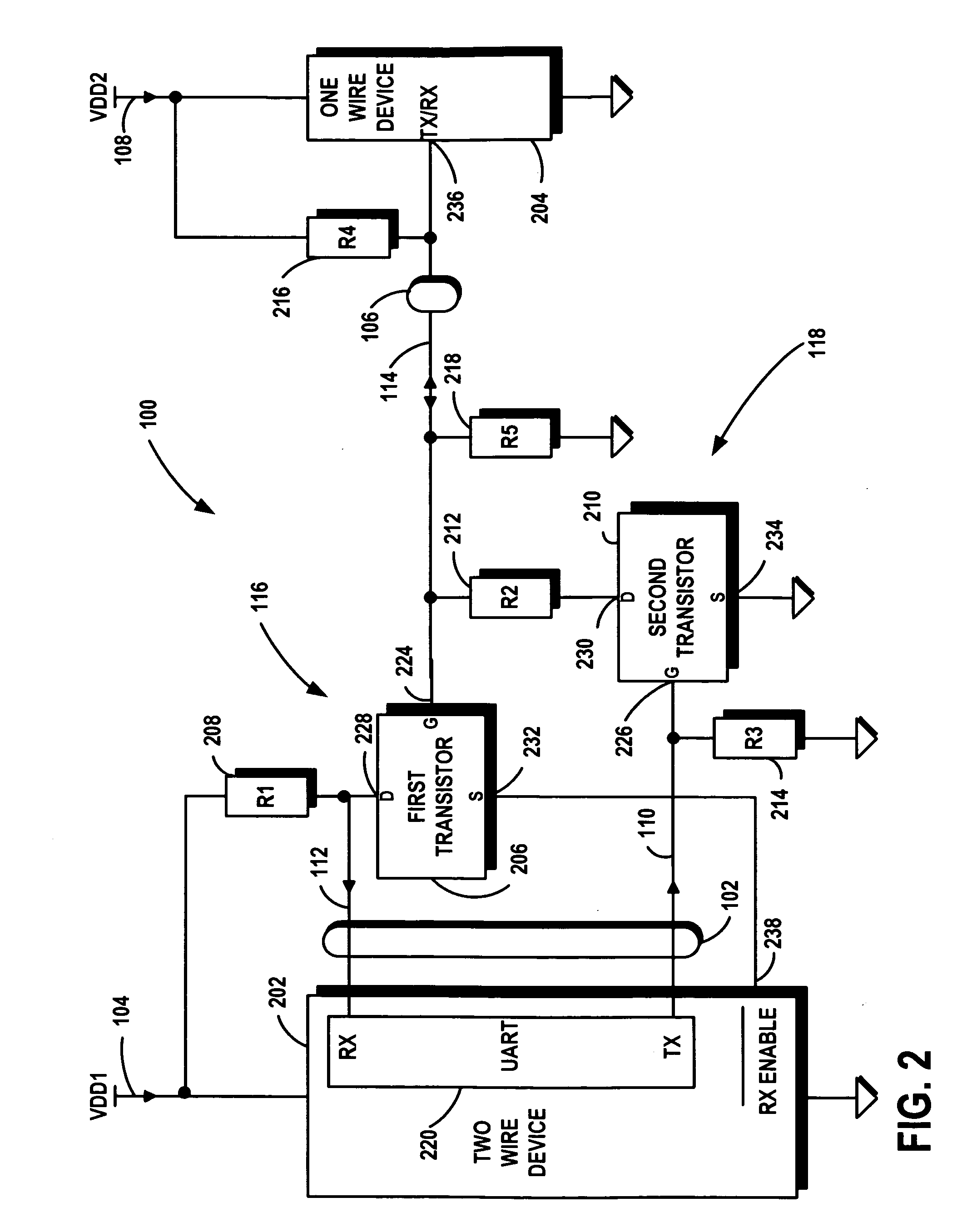
[0007]FIG. 1 is a block diagram of a level shifting multiplexing circuit connected between a two conductor full duplex bus 102 and a single conductor bidirectional bus 106 in accordance with the exemplary embodiment of the invention. The functions and operations of the blocks described in FIG. 1 may be implemented in any number of devices, circuits, or elements. Two or more of the functional blocks may be integrated in a single device and the functions described as performed in any single device may be implemented over several devices. The switching circuits include N-Channel Metal Oxide Semiconductor Field Effect Transistors (MOSFETS) and resistors in the exemplary embodiment. Although the switching circuits are represented by two blocks within the level shifting multiplexing circuit 100 in FIG. 1, some of the components of the switching circuits 116, 118 described as part of the switching circuits 116, 118 may be implemented as part of devices connected to the one of the buses 102...


PUM


Abstract

A level shifting multiplexing circuit provides an interface between a two conductor full duplex bus (two conductor bus) and a single conductor bidirectional half duplex bus (single conductor bus) where the two conductor bus is operates at a first supply voltage and the single conductor bus operates at a second supply voltage. A first switching circuit connected between the single conductor bus and the reception conductor of the two conductor bus is configured to provide a low logic signal to the reception conductor when a first switching voltage threshold is exceeded and to provide a high logic signal, otherwise. A second switching circuit connected between the single conductor bus and the transmission conductor of the two conductor bus is configured to provide a voltage less than the first switching voltage threshold when voltage at the transmission conductor exceeds a second switching voltage threshold unless a high logic signal is received on the single conductor bus. The second switching circuit is further configured to provide a voltage greater than the first switching voltage when the transmission conductor voltage exceeds the second switching voltage threshold unless a low logic signal is received on the single conductor bus.

Description

FIELD OF THE INVENTION [0001] The invention relates in general to wireless communication systems and more specifically to a level shifting multiplexing circuit for connecting a two conductor full duplex bus to a bidirectional single conductor bus. BACKGROUND OF THE INVENTION [0002] Processors exchange data over a bus to communicate with other devices and other processors. A typical arrangement includes a two wire device utilizing a universal asynchronous receiver / transmitter (UART) to communicate with one or more devices such as slave processors. A bus allows multiple devices to communicate over one or more conductors such as wires. Due to design limitations related to size, supply power, and other factors, it is often advantageous to limit the number of pins on packaged electronic devices, wires, and other conductors. A single conductor bus allows for fewer pins and conductors as compared to multiple conductor buses. Conventional designs utilizing single conductor buses, however, a...

Claims


Application Information

Patent Timeline
IPC IPC(8): H03K19/0175
CPCG06F13/4072H03K17/002H03K19/01759H04L25/0272H04L5/1461H04L5/16H04L5/14H03K19/0185G06F13/40
Inventor TAYLOR, JOHN PHILIP
Owner KYOCERA CORP
Why Eureka
Try Eureka