System and method for inspecting patterned devices having microscopic conductors
- Summary
- Abstract
- Description
- Claims
- Application Information
AI Technical Summary
Benefits of technology
Problems solved by technology
Method used
Image
Examples
Embodiment Construction
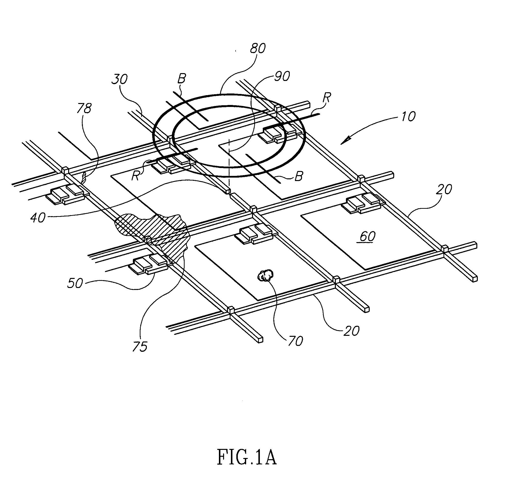
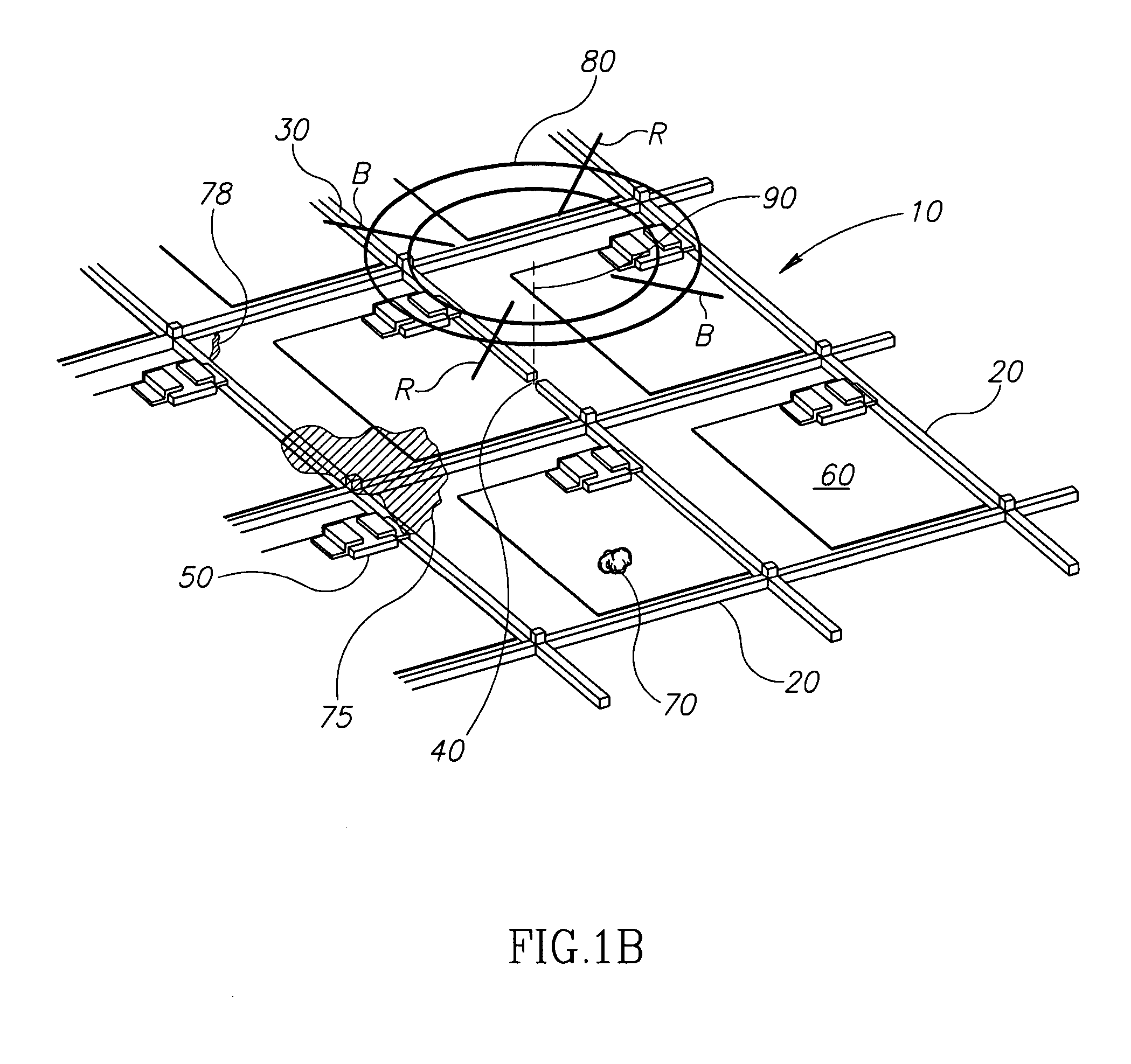
[0054]FIG. 1A is a simplified pictorial illustration of a portion of a display panel 10 including a plurality of elongate elements 20, such as electrical conductors, one of which 30 has a cut defect at defect location 40, and also includes transistors 50, electrodes 60, and other electrical components. Other defects that may appear on a display panel 10 include foreign particles 70, such as dust, which may be found on an outer surface of panel 10 or buried beneath a coating such as a photo resist (not seen), chemical residues 75, and shorts 78 forming an undesired electrical connection between two conductors 20. The display panel 10 requires inspection at defect location 40, for example in order to classify the type of defect thereat, for example as a cut, particle, short or other class of defect. The presence of a candidate defect location may be determined by initial automated inspection, for example using SuperVision™ or InVision™ automated optical inspection equipment commercial...
PUM
 Abstract
Description
Claims
Application Information
 - R&D
- Intellectual Property
- Life Sciences
- Materials
- Tech Scout
- Unparalleled Data Quality
- Higher Quality Content
- 60% Fewer Hallucinations
Browse by: Latest US Patents, China's latest patents, Technical Efficacy Thesaurus, Application Domain, Technology Topic, Popular Technical Reports.
© 2025 PatSnap. All rights reserved.Legal|Privacy policy|Modern Slavery Act Transparency Statement|Sitemap|About US| Contact US: help@patsnap.com


