Infrared sensor and infrared sensor array
a technology of infrared sensors and arrays, applied in the field of infrared sensors, can solve the problems of difficult to precisely detect the temperature of semiconductor substrates, and achieve the effect of small offset and large s/n ratio without complicating circuit configuration
- Summary
- Abstract
- Description
- Claims
- Application Information
AI Technical Summary
Benefits of technology
Problems solved by technology
Method used
Image
Examples
first embodiment
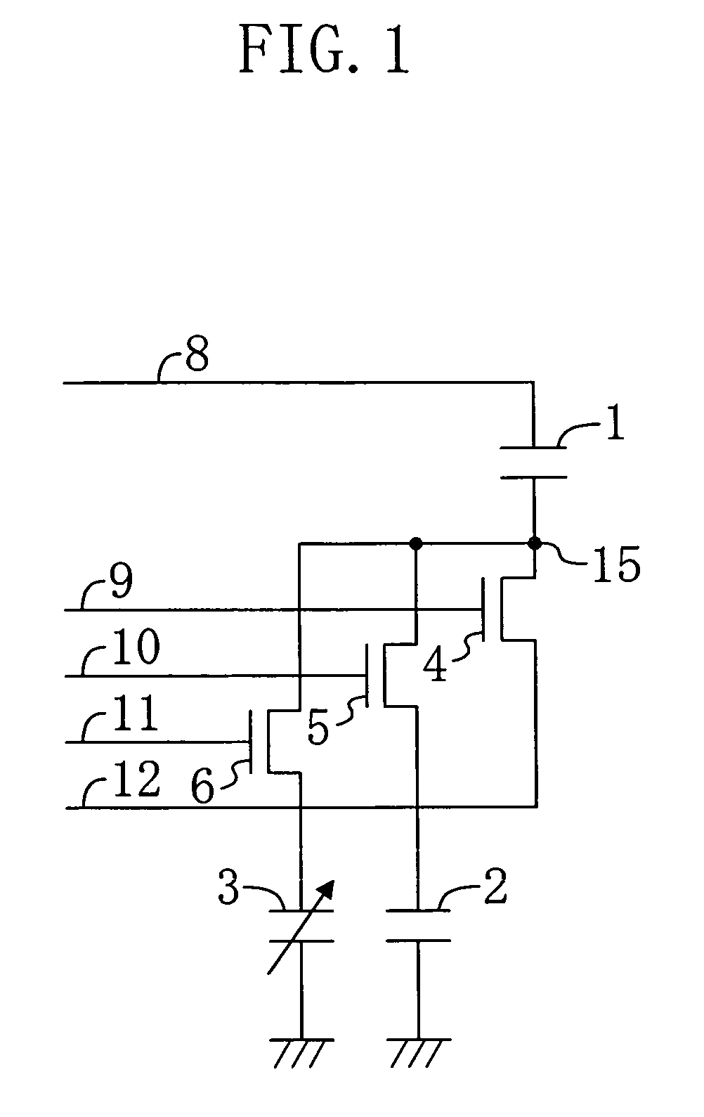
[0123] An infrared sensor according to a first embodiment of the present invention will now be described with reference to the drawings. FIG. 1 is a basic circuit diagram showing an infrared sensor of the present embodiment.
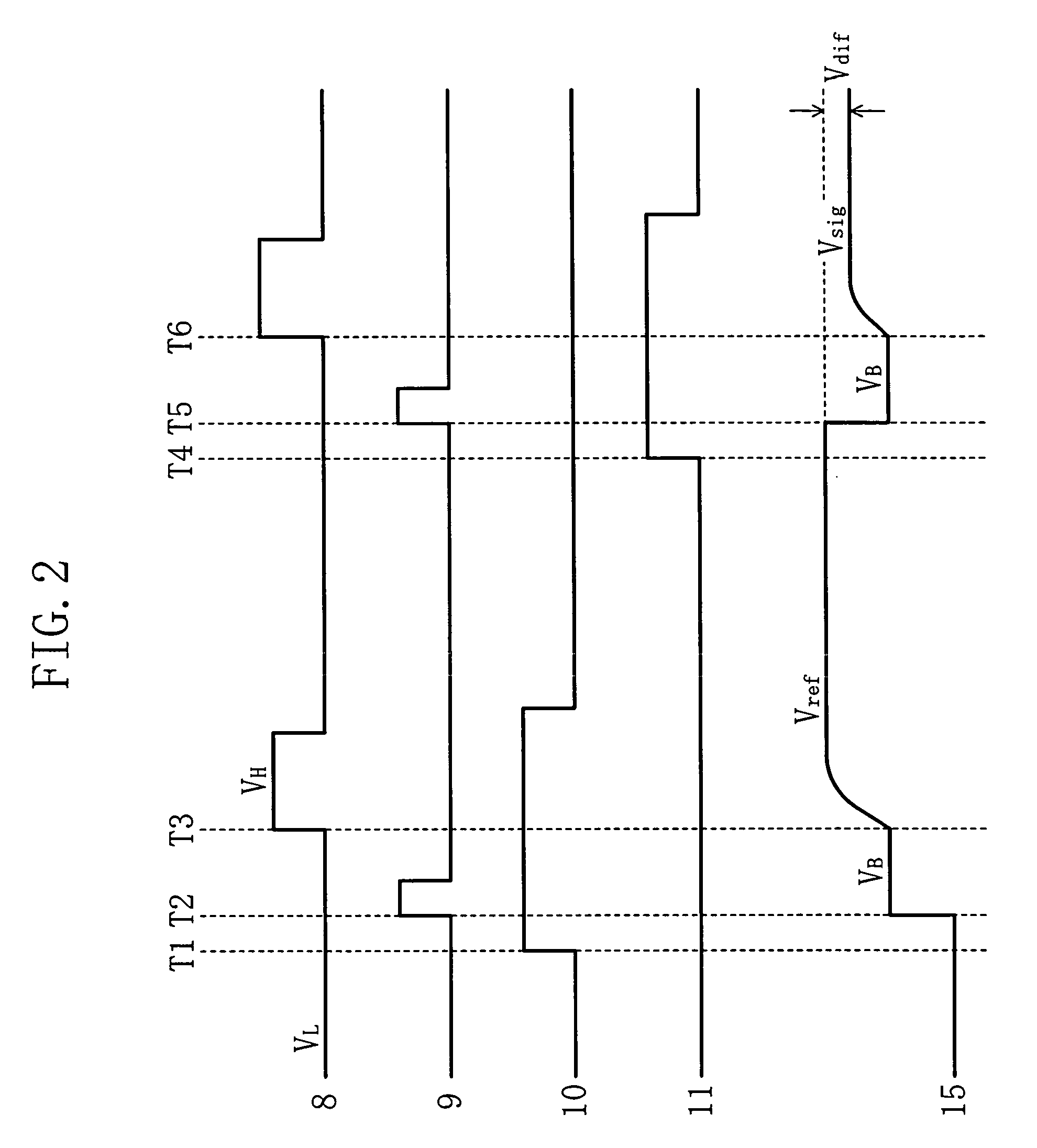
[0124] As shown in FIG. 1, in the infrared sensor of the present embodiment, a first terminal of a series capacitor element 1 is electrically connected to first terminals of a reference capacitor element 2 and an infrared-detecting capacitor element 3 via a reference capacitor element control switch 5 and an infrared-detecting capacitor element control switch 6, each being a MOS transistor, thus forming an output node 15. The capacitance value of the series capacitor element 1 and that of the reference capacitor element 2 are set so as to be substantially the same as the capacitance value of the infrared-detecting capacitor element 3 when there is no incident infrared light. Thus, these capacitance values are equal to one another within the range of their tolera...
second embodiment
[0135] A second embodiment of the present invention will now be described with reference to the drawings. FIG. 3 is a basic circuit diagram showing an infrared sensor array of the present embodiment.
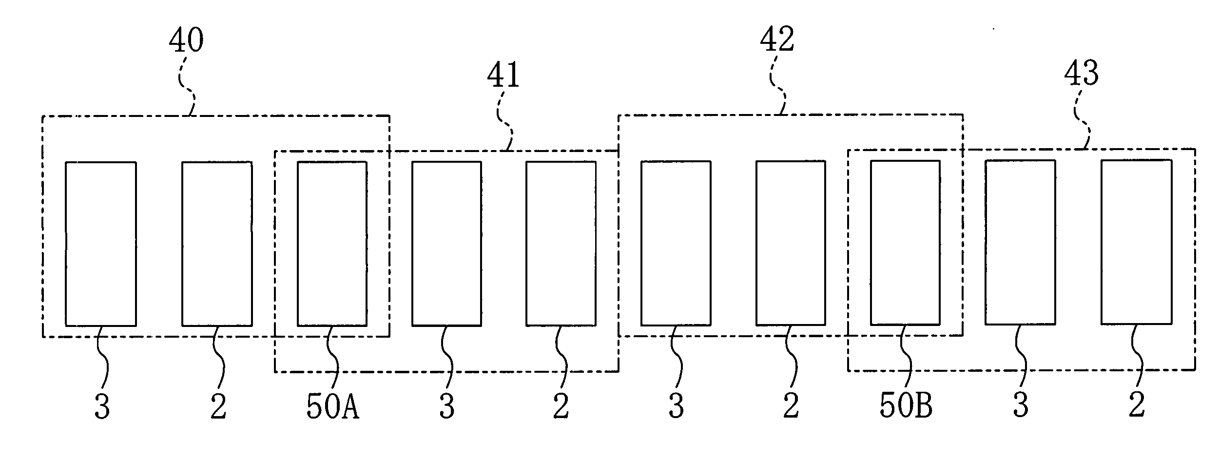
[0136] In the present embodiment, four infrared sensors, i.e., an infrared sensor 20, an infrared sensor 21, an infrared sensor 22 and an infrared sensor 23, are arranged in a matrix pattern to form an infrared sensor array, as shown in FIG. 3. The basic configuration of each infrared sensor is the same as that of the first embodiment.
[0137] The bias control lines 9, the reference capacitor element control lines 10 and the infrared-detecting capacitor element control lines 11 of the infrared sensors 20 to 23 are commonly connected to a vertical scanning and signal controlling section 28. The bias lines 12 are all connected in parallel and are connected to a bias power supply 37. The power supply lines 8 are commonly connected to the vertical scanning and signal controlling section 28 v...
third embodiment
[0149] A third embodiment of the present invention will now be described with reference to the drawings. FIG. 5 shows a basic circuit configuration of an infrared sensor of the present embodiment. As shown in FIG. 5, the infrared sensor of the present embodiment includes an output circuit 90, being an impedance conversion circuit or an amplifier circuit, provided downstream of the output node 15 shown in the first embodiment.
[0150]FIG. 6 shows a source follower circuit as an example of the output circuit 90. As shown in FIG. 6, the source follower circuit includes an MOS transistor 91 and an MOS transistor 92 connected in series with each other between the power supply and the ground. The signal from the output node 15 is input to the gate of the transistor 91, and a bias voltage is applied to the gate of the transistor 92. With such a configuration, an impedance-converted signal is output to a source follower output node 93, being the node between the transistor 91 and the transis...
PUM
 Abstract
Description
Claims
Application Information
 - R&D
- Intellectual Property
- Life Sciences
- Materials
- Tech Scout
- Unparalleled Data Quality
- Higher Quality Content
- 60% Fewer Hallucinations
Browse by: Latest US Patents, China's latest patents, Technical Efficacy Thesaurus, Application Domain, Technology Topic, Popular Technical Reports.
© 2025 PatSnap. All rights reserved.Legal|Privacy policy|Modern Slavery Act Transparency Statement|Sitemap|About US| Contact US: help@patsnap.com


