
Method for operating a data storage apparatus employing passive matrix addressing

Inactive Publication Date: 2007-05-10
THIN FILM ELECTRONICS ASA
View PDF4 Cites 11 Cited by
  • Summary
  • Abstract
  • Description
  • Claims
  • Application Information

AI Technical Summary

Benefits of technology

[0027] The principal object of the invention is to increase the possible data rate by remedying the above-mentioned problems.
[0028] Another object of the present invention is to distribute addressing operations such that the lifetime restricted by fatigue increases.

Problems solved by technology

Even though some prior art segmentation reduces the total disturb and a well designed pulse protocol in the prior art may keep disturb voltages at a low level, there are still disturb voltages present within each segment, something which in combination with the imprint phenomenon and due to occurrence of sneak and relaxation currents, makes it necessary to decrease the data rate of the memory device to assure delays between operations and active voltage pulses such that sneak and relaxation currents may decline and switched cells will get time to settle.

Method used


Image

  • Method for operating a data storage apparatus employing passive matrix addressing
  • Method for operating a data storage apparatus employing passive matrix addressing
  • Method for operating a data storage apparatus employing passive matrix addressing

Examples


Embodiment Construction

[0066] Before giving a detailed description of preferred embodiments, some of the prerequisites as well as topics of importance in the general background of the present invention shall be discussed and analysed in more detail to give a better understanding of the objects achieved by the invention.

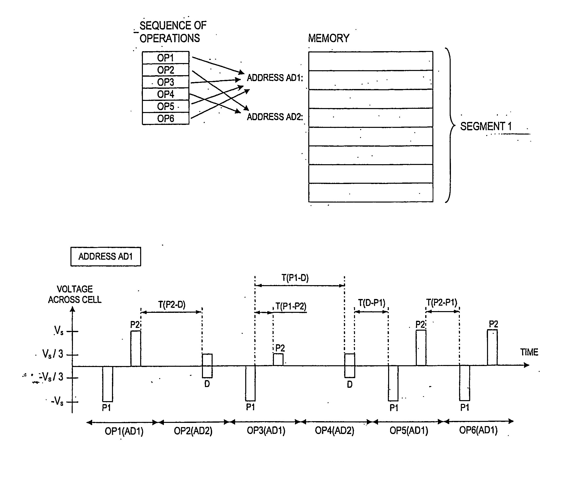
[0067]FIG. 9 shows an example of intervals negatively affecting the data rate in a passive matrix-addressable device with memory cells of polarizable material, e.g. a ferroelectric material. The intervals exemplified in FIG. 9 have been identified to contribute the most in limiting the data rate. With reference to FIG. 9, a sequence of operations on two different addresses in the same segment results in a pattern of voltage pulses at a cell at one of the addresses, address AD1. An operation on address AD1 consists of a first active voltage pulse P1 of magnitude −VS applied to each cell at the address and a second voltage pulse P2, which is either a second active voltage pulse of magnitude ...


PUM


Abstract

In a method for reducing detrimental phenomena related to disturb voltages in a data storage apparatus employing passive matrix addressing, particularly a memory device or a sensor device, an application of electric potentials conforming to an addressing operation is generally controlled in a time-coordinated manner according to a voltage pulse protocol. In an addressing operation a data storage cell is set to a first polarization state by means of a first active voltage pulse and then, dependent on the voltage pulse protocol, a second voltage pulse which may be a second active voltage pulse of opposite polarity to that of the first voltage pulse, is applied and used for switching the data storage cell to a second polarization state. The addressed cell is thus set to a predetermined polarization state as specified by the addressing operation. The data storage cells of the apparatus are provided in two or more electrically separated segments such that each segment comprises a separate physical address space for the apparatus. In an addressing operation the data are directed to a segment that is selected based on information on prior and / or scheduled applications of active voltage pulses to the segments.

Description

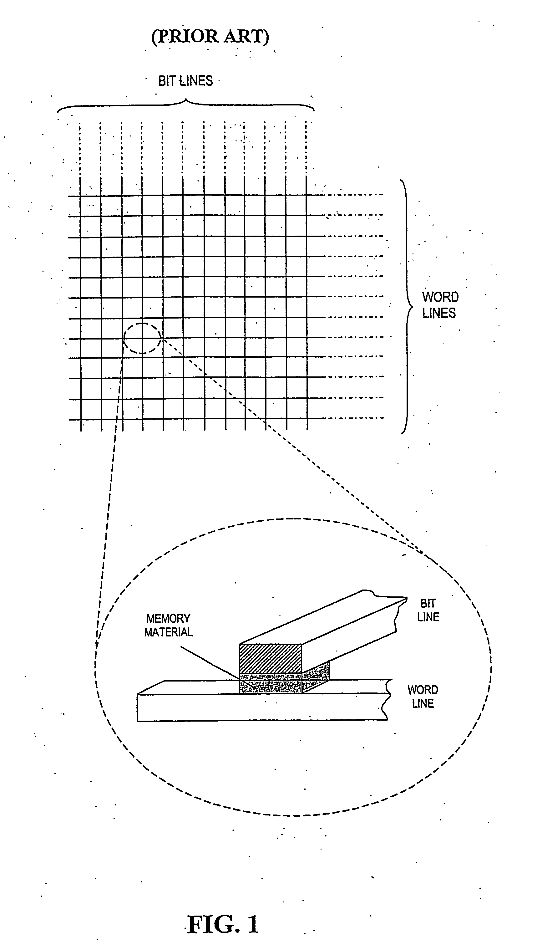
FIELD OF THE INVENTION [0001] The present invention concerns methods for reducing detrimental phenomena related to disturb voltages in a data storage apparatus employing passive matrix addressing according to the introduction of claim 1. DESCRIPTION OF THE RELATED PRIOR ART [0002] The relevant configuration as described above is well known in the prior art, and is typically referred to as a passive matrix-addressable memory. As shown in FIG. 1, it is typically implemented by letting two sets of parallel electrodes cross each other, normally in an orthogonal fashion, in order to create a matrix of cross-points that can be individually accessed electrically by selective excitation of the appropriate electrodes from the edge of the matrix. In the following, the horizontal and vertical electrodes in FIG. 1 shall be referred to as “word lines” and “bit lines”, respectively. A layer of ferroelectric or electret material is provided between or at the electrode sets such that capacitor-like...

Claims


Application Information

Patent Timeline
IPC IPC(8): G11C11/22G06F12/02G11CG11C7/02G11C8/06G11C8/12G11C8/18
CPCG06F12/0238G06F2212/1036G06F2212/7211G11C8/12G11C11/22G11C2013/0083G11C8/06
Inventor HAMBERG, PERKARLSSON, CHRISTERNORDAL, PER-ERIKOJAKANGAS, NICKLASCARLSSON, JOHANGUDESEN, HANS GUDE
Owner THIN FILM ELECTRONICS ASA
Learn More