Transflective liquid crystal display device
a liquid crystal display and transflective technology, applied in static indicating devices, instruments, non-linear optics, etc., can solve the problem of reverse contrast between the transmissive portion and the reflective portion
- Summary
- Abstract
- Description
- Claims
- Application Information
AI Technical Summary
Benefits of technology
Problems solved by technology
Method used
Image
Examples
embodiment 1
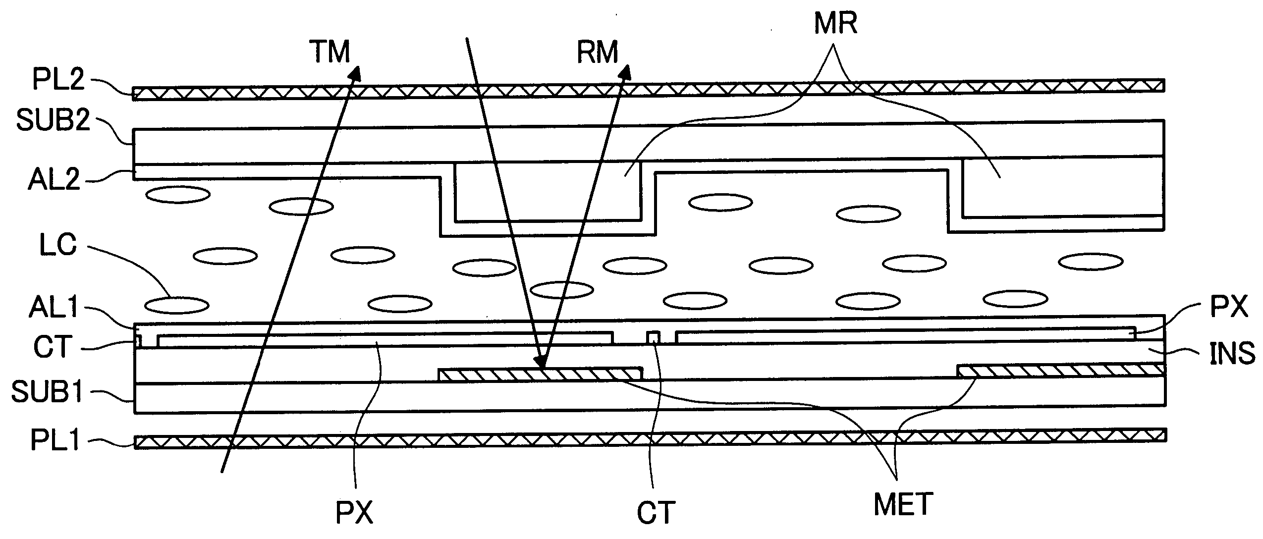
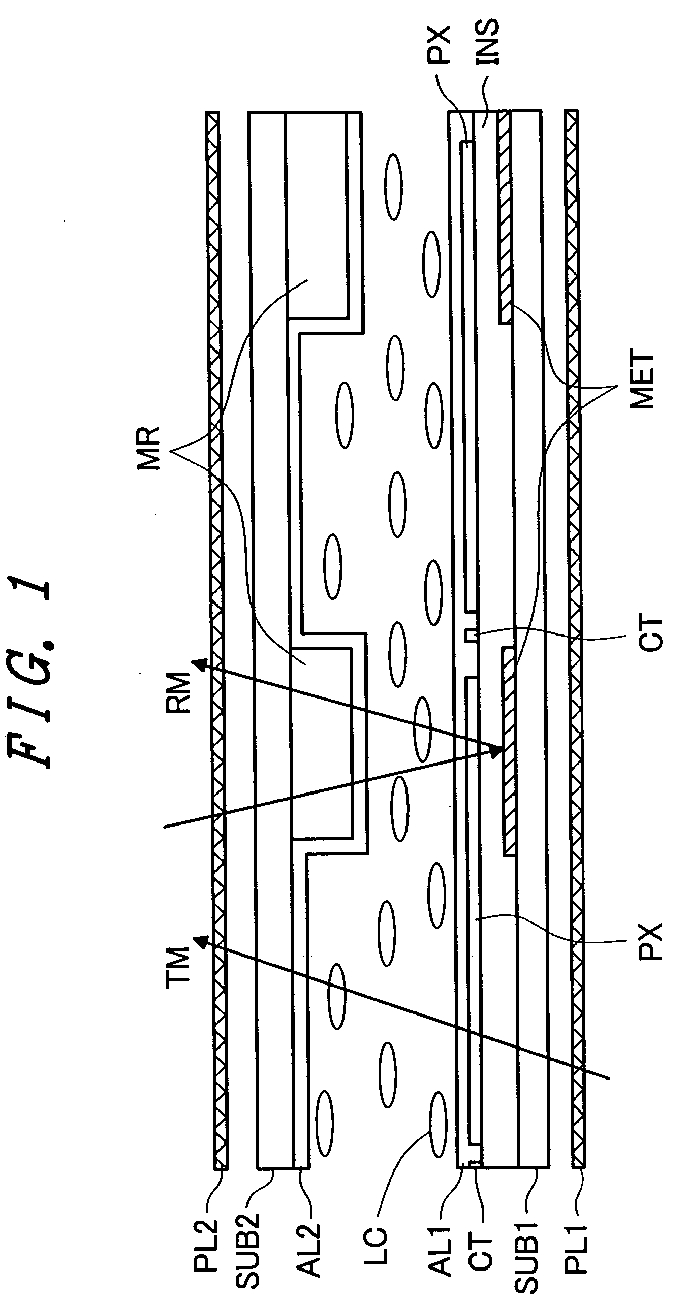
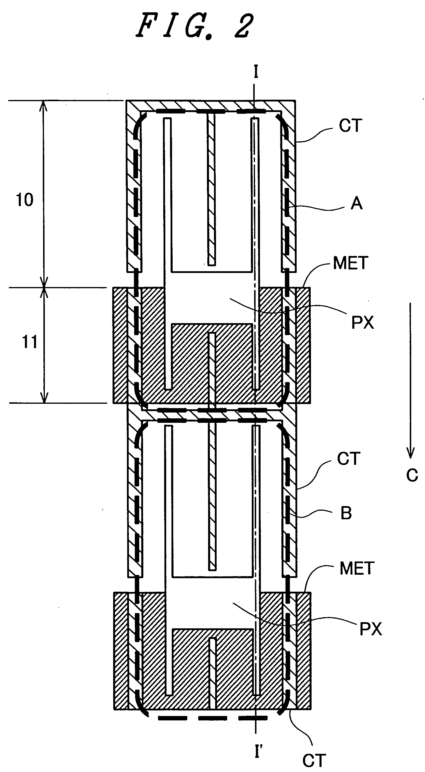
[0060]FIG. 1 is a cross-sectional view of an essential part showing the schematic constitution of a sub pixel of a transflective liquid crystal display device according to an embodiment 1 of the present invention, while FIG. 2 is a plan view showing the electrode structure of the sub pixel of the transflective liquid crystal display device according to the embodiment 1 of the present invention. Here, FIG. 1 is a cross-sectional view taken along a line I-I′ in FIG. 2.
[0061] Hereinafter, the transflective liquid crystal display device of this embodiment is explained in conjunction with FIG. 1 and FIG. 2.
[0062] As shown in FIG. 1, in this embodiment, a pair of glass substrates (SUB1, SUB2) are provided in a state that a liquid crystal layer (LC) is sandwiched between the pair of glass substrates (SUB1, SUB2).
[0063] On one glass substrate (SUB1), for example, a reflective layer (MET) made of Al, an interlayer insulation film (INS) which is formed on the reflective layer (MET), pixel ...
embodiment 2
[0096]FIG. 6 is a cross-sectional view of an essential part showing the schematic constitution of a sub pixel of a transflective liquid crystal display device according to an embodiment 2 of the present invention, and FIG. 7 is a plan view showing the electrode structure of the sub pixel of the transflective liquid crystal display device of this embodiment. Here, FIG. 6 is a cross-sectional view taken along a line I-I′ in FIG. 7.
[0097] In the previously mentioned embodiment 1, the pixel electrodes (PX) and the counter electrodes (CT) in the transmissive portion 10 and the reflective portion 11 are formed on the same layer on one substrate (SUBI) and, at the same time, both of the pixel electrodes (PX) and the counter electrodes (CT) are not overlapped to each other.
[0098] On the other hand, this embodiment differs from the above-mentioned embodiment with respect to the point that the pixel electrodes (PX) and the counter electrodes (CT) of the transmissive portion 10 and the refle...
PUM
| Property | Measurement | Unit |
|---|---|---|
| reflectance | aaaaa | aaaaa |
| electric field | aaaaa | aaaaa |
| voltage | aaaaa | aaaaa |
Abstract
Description
Claims
Application Information
 - R&D
- Intellectual Property
- Life Sciences
- Materials
- Tech Scout
- Unparalleled Data Quality
- Higher Quality Content
- 60% Fewer Hallucinations
Browse by: Latest US Patents, China's latest patents, Technical Efficacy Thesaurus, Application Domain, Technology Topic, Popular Technical Reports.
© 2025 PatSnap. All rights reserved.Legal|Privacy policy|Modern Slavery Act Transparency Statement|Sitemap|About US| Contact US: help@patsnap.com


