Semiconductor memory chip with on-die termination function
a memory chip and on-die termination technology, applied in the field of semiconductor memory chips, can solve problems such as the synchronous input buffer might malfunction
- Summary
- Abstract
- Description
- Claims
- Application Information
AI Technical Summary
Problems solved by technology
Method used
Image
Examples
first embodiment
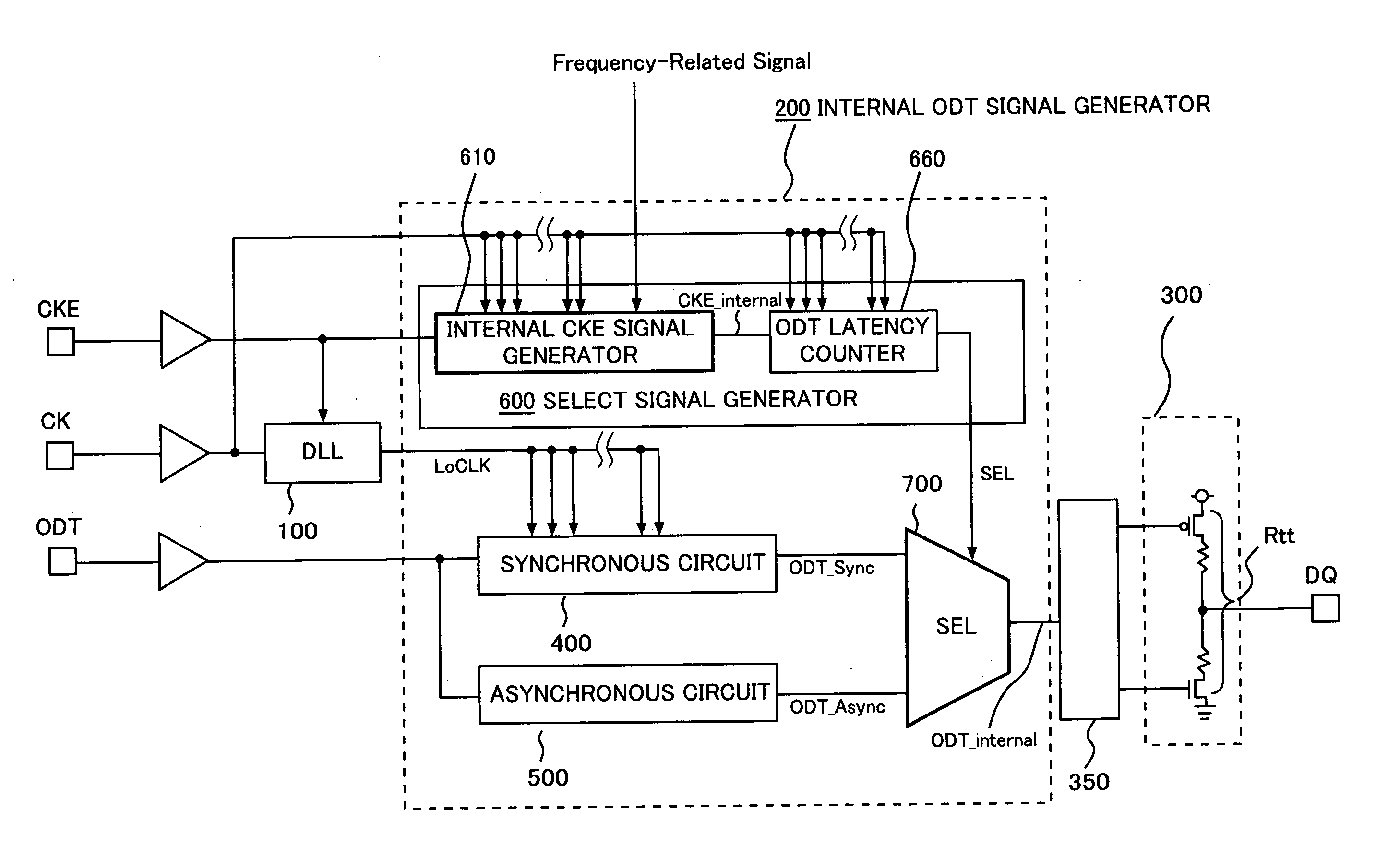
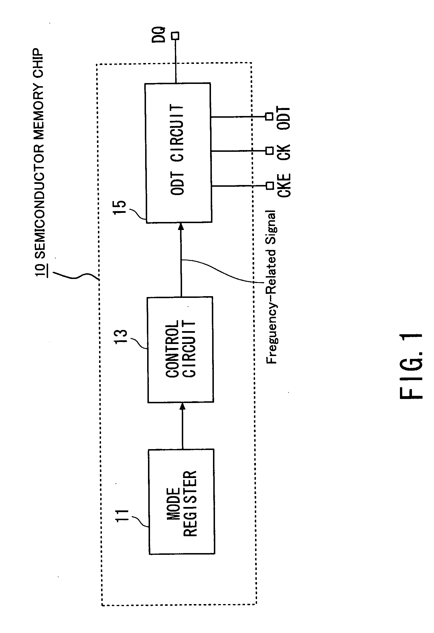
[0014] With reference to FIG. 1, a semiconductor memory chip 10 according to the present invention is a dynamic random access memory (DRAM) chip and comprises a mode register 11, a control circuit 13 and an ODT circuit 15.
[0015] The mode register 11 stores a predetermined value associated with a predetermined frequency at which the semiconductor memory chip 10 is used. For example, the semiconductor memory chip 10 of the present embodiment can be used at four different kinds of predefined frequencies, i.e. 400 MHz, 533 MHz, 667 MHZ, 800 MHz. The predetermined frequency is an actually-used one of the predefined frequencies. The mode register may include an extended mode register.
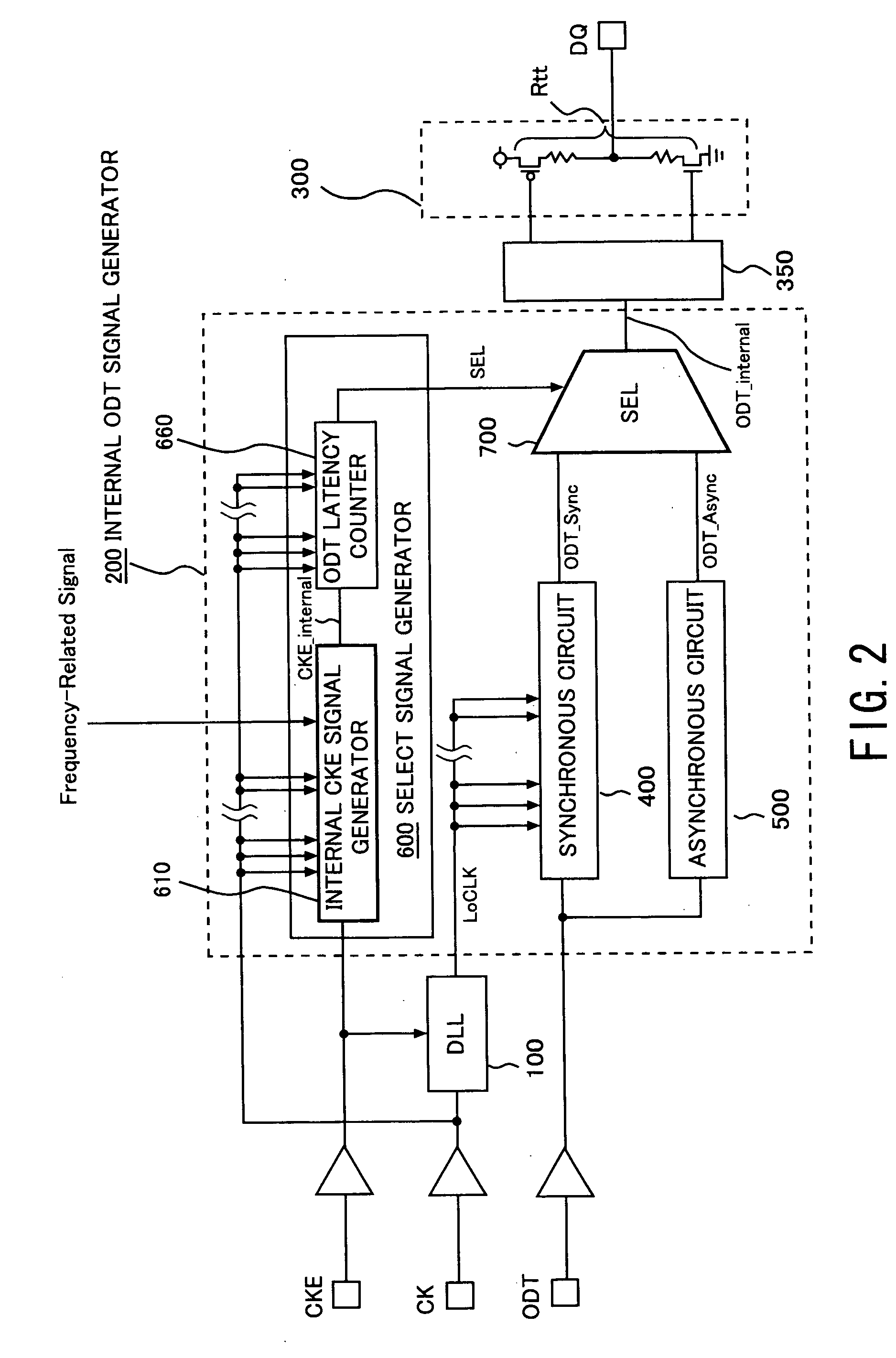
[0016] The control circuit 13 produces a frequency-related signal on the basis of the predetermined value stored in the mode register 11. The frequency-related signal implies the predetermined frequency. In other words, the frequency-related signal is for notifying which is the predetermined frequency among ...
second embodiment
[0036] With reference to FIG. 6, the delayed signal generator 645 included in the delay circuit 635 comprises a plurality of delay elements 6461 to 6463 connected in series and a plurality of taps 647. Each tap 647 is connected to one of output portions of the delay elements 6461 and 6462. The delay elements 6461, 6462, 6463 provide delay periods d1, d2−d1, and d3−(d1+d2), respectively. The taps 647 and the output portion 648 of the last stage of the delay element 6463 output the delayed signals 10 tCK+d1, 10 tCK+d2, and 10 tCK+d3, respectively. The differences d1, d2, d3 relative to 10 tCK are determined in consideration of the operation frequency of 533 MHz, 667 MHz and 800 MHz, respectively.
[0037] Although the frequency-related signal is produced on the basis of the predetermined value stored in the mode register 11 in the above-described embodiments, the frequency-related signal may be directly supplied from the outside of the semiconductor memory chip or may be produced inside...
PUM
 Abstract
Description
Claims
Application Information
 - R&D
- Intellectual Property
- Life Sciences
- Materials
- Tech Scout
- Unparalleled Data Quality
- Higher Quality Content
- 60% Fewer Hallucinations
Browse by: Latest US Patents, China's latest patents, Technical Efficacy Thesaurus, Application Domain, Technology Topic, Popular Technical Reports.
© 2025 PatSnap. All rights reserved.Legal|Privacy policy|Modern Slavery Act Transparency Statement|Sitemap|About US| Contact US: help@patsnap.com


