Organic electroluminescence device and electron transporting layer

an electroluminescence device and electron transport technology, applied in the field of luminescence devices, can solve the problems of electroluminescence devices, non-equilibrium of carriers, and low light-emitting efficiency, and achieve the effect of enhancing carrier non-equilibrium problems and electron mobility

Inactive Publication Date: 2007-05-10
CHUNGHWA PICTURE TUBES LTD
View PDF4 Cites 0 Cited by
  • Summary
  • Abstract
  • Description
  • Claims
  • Application Information

AI Technical Summary

Benefits of technology

[0008] Accordingly, the present invention is directed to provide an organic electroluminescence device that has a higher light-emitting efficiency.
[0020] Based on the above description, as the electron transportation layer of the present invention is constituted by a stacked super-lattice structure of the first sub-transportation layers and the second sub-transportation layers, the electron mobility of the electron transportation layer can be promoted and thus ameliorates the carrier transportation non-equilibrium problem occurred in the conventional organic electroluminescence device.

Problems solved by technology

Among the convention technologies, material of the electron transportation layer 150 is usually Alq3; however, since an electron mobility in Alq3 is smaller than a hole mobility in the hole transportation layer, there exists an carrier transportation non-equilibrium problem in the conventional organic electroluminescence device 100, and this problem in turn affects the organic electroluminescence device 100's light-emitting efficiency.

Method used


Image

  • Organic electroluminescence device and electron transporting layer
  • Organic electroluminescence device and electron transporting layer
  • Organic electroluminescence device and electron transporting layer

Examples


Embodiment Construction

[0026] Reference will now be made in detail to the present preferred embodiments of the invention, examples of which are illustrated in the accompanying drawings.

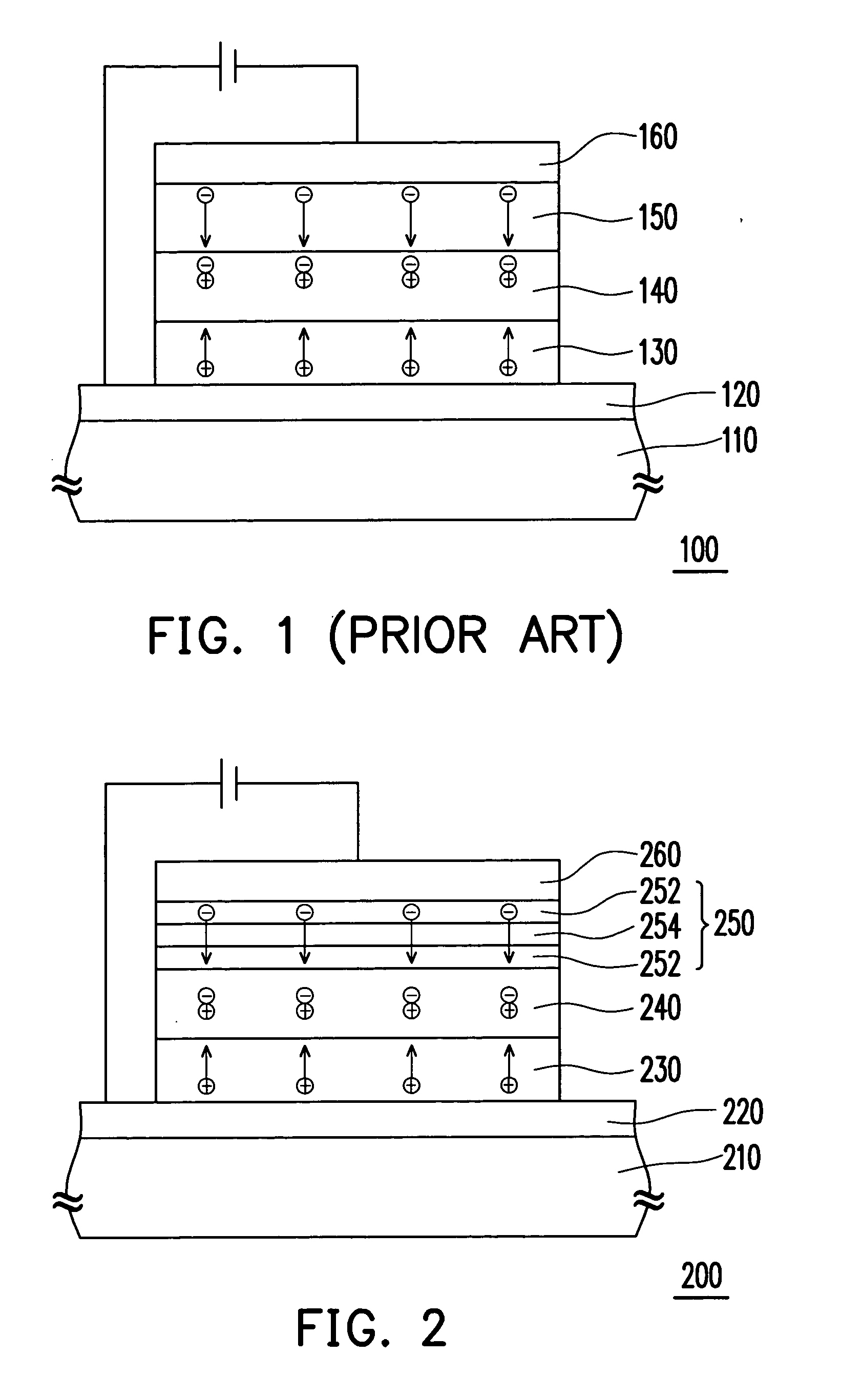
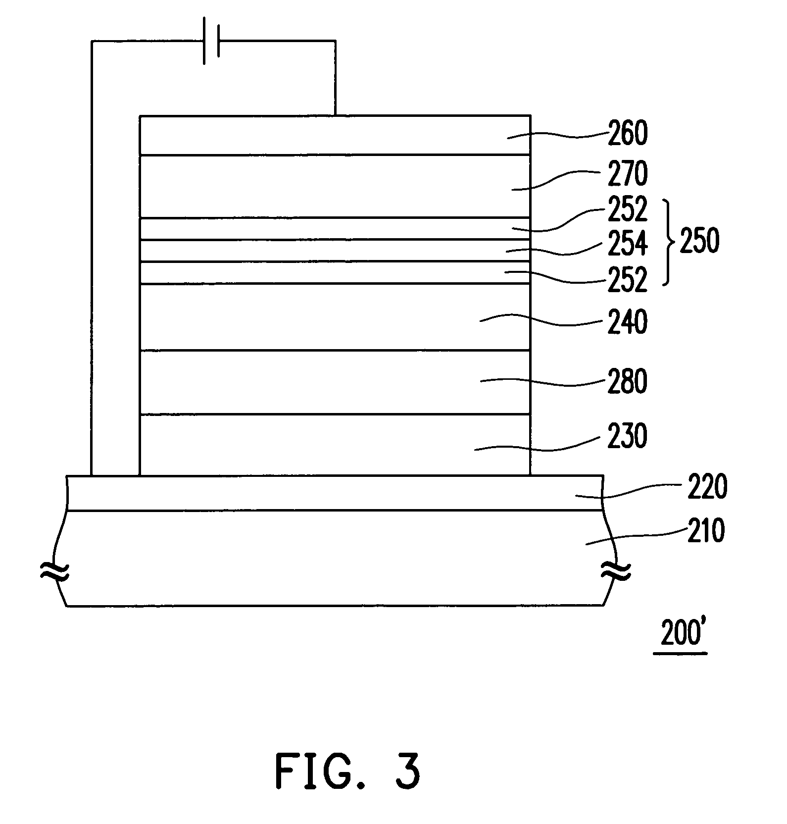
[0027]FIG. 2 schematically shows an organic electroluminescence device structure of one embodiment of the present invention. Referring to FIG. 2, an organic electroluminescence device 200 of this embodiment comprises a substrate 210, a first electrode layer 220, a hole transportation layer 230, a luminescence layer 240, an electron transportation layer 250 and a second electrode layer 260. In addition, on the substrate 210 is disposed the first electrode layer 220 on which the hole transportation layer 230 is disposed. Moreover, on the hole transportation layer 230 is disposed the luminescence layer 240 on which the electron transportation layer 250 is further disposed, and eventually, the second electrode layer 260 is disposed on the electron transportation layer 250. Moreover, the electron transportation layer 250 compri...


PUM

PropertyMeasurementUnit
Thicknessaaaaaaaaaa
Thicknessaaaaaaaaaa
Thicknessaaaaaaaaaa

Abstract

An organic electroluminescence device comprises a substrate, a first electrode layer, a hole transportation layer, a luminescence layer, an electron transportation layer and a second electrode layer. In addition, on the substrate is disposed the first electrode layer on which the hole transportation layer is further disposed. In addition, on the hole transportation layer is disposed the luminescence layer on which the electron transportation layer is further disposed, and eventually the second electrode layer is disposed on the electron transportation layer. Moreover, the electron transportation layer comprises n+1 first sub-transportation layers and n second sub-transportation layers, wherein n is an integer. The n+1 first sub-transportation layers are stacked on the luminescence layer, each of the n second sub-transportation layers is disposed between every two neighbor first sub-transportation layers and a band-gap of the first sub-transportation layer is different from that of second sub-transportation layer.

Description

BACKGROUND OF THE INVENTION [0001] 1. Field of the Invention [0002] The present invention generally relates to a luminescence device, and more particularly to, an organic electroluminescence device and an electron transportation layer thereof. [0003] 2. Description of Related Art [0004] Displays are communication interfaces between human and information processors, and have current trends in planar displays. Among displays, an organic electroluminescence display (OLED) is believed to be a main stream of the next generation planar displays because it has advantages of self-luminescence, free-viewing angle, low power consumption, easy fabrication, low cost, low operating temperature range, high response speed and full-colorized display. [0005] The OLED mainly utilizes a self-luminescence feature of the organic electroluminescence device to achieve a display effect. In addition, the organic electroluminescence device is comprised of a pair electrodes and an organic material layer. When...

Claims


Application Information

Patent Timeline
IPC IPC(8): H01L51/54
CPCY10T428/24942H01L51/5052H10K50/165
Inventor TSAI, YA-PINGCHI, CHIH-HSIENTANG, SHUENN-JIUNWU, JIE-HUANG
Owner CHUNGHWA PICTURE TUBES LTD
Why Eureka
Try Eureka