Sphere-supported thin film phosphor electroluminescent devices

a phosphor electroluminescent and sphere-supported technology, applied in solid-state devices, discharge tubes/lamp details, light sources, etc., can solve the problems of difficult formation of high dielectric constant insulating jayers, not all materials offer sufficient chemical stability and compatibility in the presence of high processing temperatures

Inactive Publication Date: 2007-03-29
NANOLUMENS ACQUISITION
View PDF11 Cites 15 Cited by
  • Summary
  • Abstract
  • Description
  • Claims
  • Application Information

AI Technical Summary

Problems solved by technology

These dielectrics do not always provide optimum EL performance due to their relatively low dielectric constants.
While all of these dielectrics exhibit a sufficiently high figure of merit (defined as the product of the breakdown electric field and the relative dielectric constant) to function in the presence of high electric fields, not all of these materials offer sufficient chemical stability and compatibility in the presence of high processing temperatures that may be required to fabricate an EL device.
Also, it is difficult to form high dielectric constant insulating jayers as thin films with good breakdown protection.
Although, due to their thickness, these dielectrics offer good breakdown protection, they limit the processing temperature of phosphors that are on top of the dielectric layer, and phosphors that require processing temperatures of 700° C. or higher may be contaminated by the dielectric formulation at these temperatures.
Also, substrate cost is much higher for ceramics than for glass, particularly for large size ceramics over ˜30 cm in length or width, since cracking and warping of large ceramic sheets is hard to control.
), warping or compaction of the glass will occur, particularly if longer annealing time are required.
During operation, these Cu2−xS tips lose their sharpness, and the electric field decreases, resulting in weaker luminescence.

Method used


Image

  • Sphere-supported thin film phosphor electroluminescent devices
  • Sphere-supported thin film phosphor electroluminescent devices
  • Sphere-supported thin film phosphor electroluminescent devices

Examples


Embodiment Construction

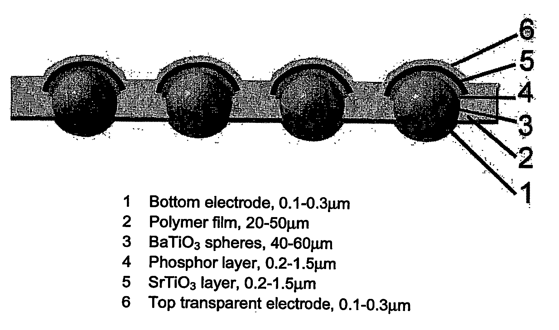
[0060] The inventors have shown for the first time that thin film phosphor electroluminescent devices can be prepared using dielectric spheres, preferably BaTiO3 spheres for electroluminescent (EL) display applications. The device possesses a novel structure and is prepared through a special processing route in order to perform high temperature annealing processes required before applying the spheres into a low temperature substrate.

[0061]FIG. 5 shows the schematic diagram of the proposed structure of the Sphere-Supported Thin Film Electroluminescent (SSTFEL) device. A phosphor layer 4 is deposited onto the top surface of BaTiO3 spheres 3. In a preferred embodiment a thin SrTiO3 layer 5 is deposited onto the phosphor layer for effective charge injection into the phosphor layer. The BaTiO3 spheres are embedded within a polymer layer 2 with the top and bottom areas of the BaTiO3 spheres exposed. The top area of the BaTiO3 spheres and the surrounding polymer is coated with transparent...


PUM

PropertyMeasurementUnit
relative permittivityaaaaaaaaaa
diameteraaaaaaaaaa

Abstract

The present invention provides an electroluminescent display device using dielectric spheres embedded in a flexible electrically conducting substrate. Each of the spherical dielectric particles has a first portion protruding through a top surface of the substrate and a second portion protruding through the bottom surface of the substrate. An electroluminescent phosphor layer is deposited on the first portion of each spherical dielectric particles and a continuous electrically conductive, substantially transparent electrode layer is located on the top surfaces of the electroluminescent phosphor layer and areas of the flexible electrically insulating substrate located between the top surfaces of the electroluminescent phosphor layer. A continuous electrically conductive electrode layer coated on the second portion of the spherical dielectric particles and areas of the flexible, electrically insulated substrate located between the second portions of the spherical dielectric particles.

Description

CROSS REFERENCE TO RELATED U.S. PATENT APPLICATION [0001] This patent application claims the priority benefit from U.S. Provisional Patent Application Ser. No. 60 / 500,375 filed on Sep. 5, 2003 entitled SPHERE-SUPPORTED THIN FILM PHOSPHOR ELECTROLUMINESCENT DEVICES, and which is incorporated herein in its entirety.FIELD OF THE INVENTION [0002] The present invention relates to materials and structures for thin film electroluminescent devices, and more particularly the present invention relates to sphere-supported thin film phosphor electroluminescent (SSTFEL) devices. BACKGROUND OF THE INVENTION [0003] Thin film electroluminescent (TFEL) devices typically consist of a laminar stack of thin films deposited on an insulating substrate. The thin films include a transparent electrode layer and an electroluminescent (EL) layer structure, comprising an EL phosphor material sandwiched between a pair of insulating layers. A second electrode layer completes the laminate structure. In matrix add...

Claims


Application Information

Patent Timeline
Patent Type & Authority Applications(United States)
IPC IPC(8): H01J1/62C04B35/44C04B35/468C04B35/547C09K11/59C09K11/62C09K11/66C09K11/77G09F9/33H01L25/075H01L29/00H01L33/00H05B33/14H05B33/22H05B33/26
CPCC04B35/01H05B33/26C04B35/44C04B35/4682C04B35/547C04B2235/3205C04B2235/3208C04B2235/3215C04B2235/3217C04B2235/3224C04B2235/3262C04B2235/3284C04B2235/3286C04B2235/3287C04B2235/3418C04B2235/528C04B2235/5436C09K11/595C09K11/621C09K11/662C09K11/666C09K11/7734H01L25/0753H05B33/22C04B35/16H01L2924/0002H01L2924/00
Inventor KITAI, ADRIANXIANG, YING-WEICOX
Owner NANOLUMENS ACQUISITION
Why Eureka
Try Eureka