Aluminum sputtering while biasing wafer

a technology of biasing wafers and aluminum sputtering, which is applied in the direction of vacuum evaporation coatings, electrolysis components, coatings, etc., can solve the problems of large unbalanced magnetron, large unbalanced magnetron, and general isotropic flux pattern of neutral sputter atoms unsuitable for filling high aspect-ratio holes

Inactive Publication Date: 2007-03-01
APPLIED MATERIALS INC
View PDF11 Cites 28 Cited by
  • Summary
  • Abstract
  • Description
  • Claims
  • Application Information

AI Technical Summary

Benefits of technology

[0021] The blanket thickness of the seed layer relative to the fill layer measured on the top planar surface should be less than that of the fill layer and preferably

Problems solved by technology

However, as the aspect ratio of vertical interconnects continues to increase, a geometry generally unfavorable for sputtering, aluminum sputtering faces increased challenges.
SIP sputtering relies upon high target power, high wafer biasing, and a relatively small unbalanced magnetron.
A conventional aluminum sputter coating using the Tepman magnetron of FIG. 3 and an unbiased wafer, however produces a generally isotropic flux pattern of neutral sputter atoms unsuitable for filling high aspect-ratio holes.
In particular, overhangs 112 tend to develop at the top corners of th

Method used


Image

  • Aluminum sputtering while biasing wafer
  • Aluminum sputtering while biasing wafer
  • Aluminum sputtering while biasing wafer

Examples


Embodiment Construction

[0029] In one aspect of the invention and, illustrated in the cross-sectional view of an aluminum metallization structure in FIG. 5, an aluminum sputter fill process is divided into the sputter deposition of a thin aluminum seed layer 120 and a subsequent sputter deposition of a thicker aluminum fill layer 122. The deposition of these two different layers 120, 122 having significantly different characteristics is achieved by a significant change of the sputtering conditions between the two steps.

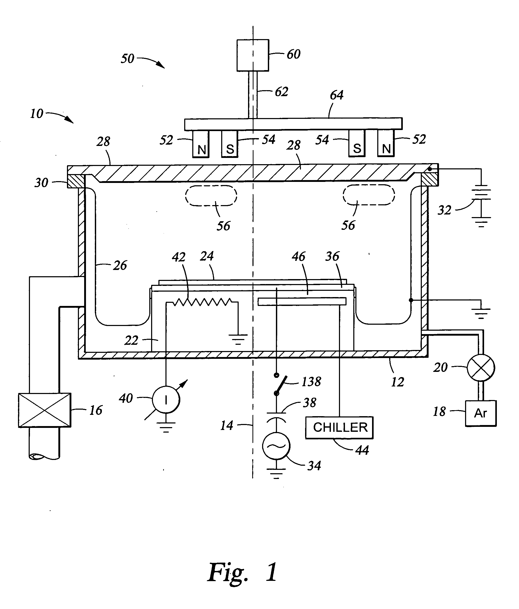
[0030] A broad aspect of the invention includes a cold, biased sputter deposition process for depositing aluminum, for example, to form the thin, nearly conformal seed layer 120 deep within a narrow hole while the wafer 106 is biased negatively to draw ionized aluminum sputter atoms deep within the hole and also while the wafer 106 is maintained at a relatively low temperature so that the aluminum sputter atoms stick to the barrier layer 108 on the hole sidewalls.

[0031] The cold, biased al...


PUM

PropertyMeasurementUnit
Temperatureaaaaaaaaaa

Abstract

An aluminum sputtering process including RF biasing the wafer and a two-step aluminum fill process and apparatus used therefor to fill aluminum into a narrow via hole by sputtering under two distinctly different conditions, preferably in two different plasma sputter reactors. The first step includes sputtering a high fraction of ionized aluminum atoms onto a relatively cold wafer, e.g., held at less than 150° C., and relatively highly biased to attract aluminum atoms into the narrow holes and etch overhangs. The second step includes more neutral sputtering onto a relatively warm wafer, e.g. held at greater than 250° C., and substantially unbiased to provide a more isotropic and uniform aluminum flux. The magnetron scanned about the back of the aluminum target may be relatively small and unbalanced in the first step and relatively large and balanced in the second.

Description

FIELD OF THE INVENTION [0001] The invention relates generally to deposition of materials by sputtering. In particular, the invention relates to a two-step aluminum sputtering process and apparatus used therefor. BACKGROUND ART [0002] Silicon integrated circuits continue to often use aluminum as the conductive material for vertical and horizontal interconnects in a multi-level metallization structure despite an increased emphasis on copper metallization for very advanced circuitry. The aluminum is most often deposited by magnetron sputtering. However, as the aspect ratio of vertical interconnects continues to increase, a geometry generally unfavorable for sputtering, aluminum sputtering faces increased challenges. Nonetheless, relatively conventional DC magnetron sputter reactors continue to be favored because of their simplicity, low cost, and long usage. [0003] As schematically illustrated in the cross sectional view of FIG. 1, a DC magnetron sputter reactor 10 includes a vacuum ch...

Claims


Application Information

Patent Timeline
IPC IPC(8): C23C14/00
CPCC23C14/025C23C14/046C23C14/185C23C14/345C23C14/081C23C14/541
Inventor LEE, WEI TIGUO, TEDYU, SANG-HO
Owner APPLIED MATERIALS INC
Why Eureka
Try Eureka