Antenna switch module

Active Publication Date: 2007-01-25
STMICROELECTRONICS SRL
View PDF6 Cites 4 Cited by
  • Summary
  • Abstract
  • Description
  • Claims
  • Application Information

AI Technical Summary

Benefits of technology

[0024] The present invention also aims at providing a solution avoiding simultaneous use of positive and negative bias voltages on the diodes.

Problems solved by technology

Conversely, when they are reverse-biased or even at 0 V, due to their low capacitance, the diodes block the RF signals.
A disadvantage of circuits combining high-frequency diodes and quarter-wave impedances is that they require many passive elements and many diodes, which increases the bulk.
Another disadvantage is that the presence of the quarter-wave impedances in series increases insertion losses of the antenna switch module.
However, a disadvantage is that each blocked diode (and thus four diodes out of five in the example of FIG. 2) generates harmonics of order 2 having non-negligible amplitudes when the selected path is a transmit path.
This however increases switch insertion losses.
This however requires negative and positive bias voltages, while the two biasings are not necessarily available in the concerned devices.

Method used


Image

  • Antenna switch module
  • Antenna switch module
  • Antenna switch module

Examples


second embodiment

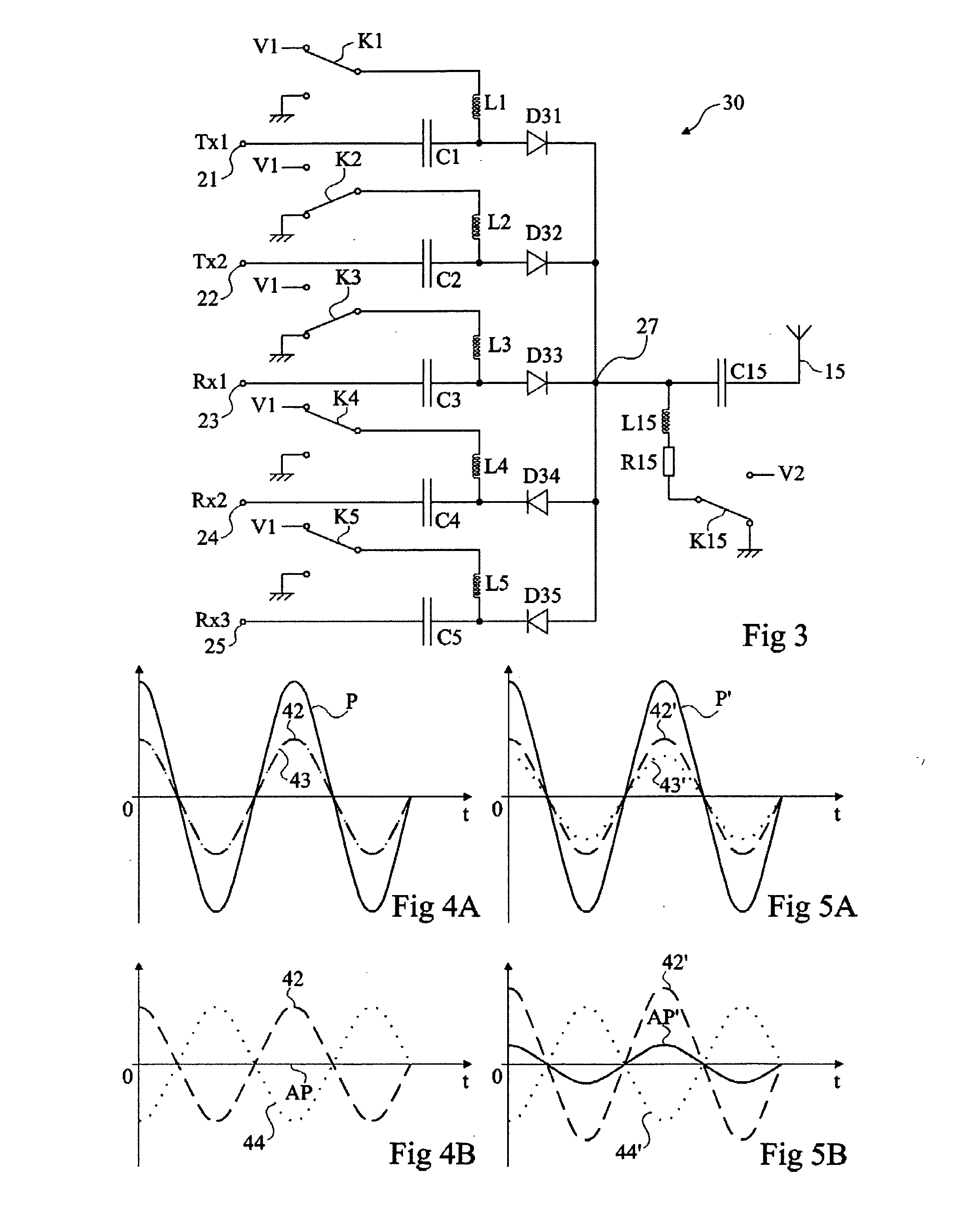
[0057]FIG. 6 shows an antenna switch module 60 according to the present invention intended to switch six paths. The first five paths of FIG. 3 (with diodes designated by D61 to D65), to which a path Rx4 (terminal 26, capacitor C6, diode D66, bias circuit L6, K6) has been added, are shown. Since the total number of paths is even, a fictitious path which introduces an additional diode D67 is added to respect the previously-discussed condition. Thus, in this example, the four diodes D51 to D64 have their cathodes interconnected, while three diodes D65 to D67 have their anodes interconnected, diode D67 having its cathode connected, for example to ground by a normalization impedance Z (generally 50Ω) in series with a capacitor C7. The cathode of diode D57 is always biased to voltage V1 since it must remain blocked. An optional switch K7 has however been shown.

[0058] In the example of FIG. 6, it is assumed that the selected path is path Tx2. The ground is selected by switch K15 and voltag...

third embodiment

[0060]FIG. 7 shows the present invention in which antenna switch 70 is said to be “in cascade”, that is, a group of paths (for example, receive paths Rx1 to Rx4) has a common diode D78 between an interconnection point 77 of the cathodes of diodes D73 to D76 of the individual paths and common terminal 27 of the switch on the antenna side. In this example, transmit paths Tx1 and Tx2 have diodes D71 and D72 having their anodes interconnected to terminal 27. This embodiment also enables providing an even number of paths by saving, with respect to the solution of FIG. 6, a bias circuit and a capacitor (fictive path).

[0061] As a variation, an additional diode in the same direction as diodes D71 and D72 may be interposed between the common anodes of diodes D71 and D72 and terminal 27 and create a second group, provided for an additional fictive path (diode 67, FIG. 6) to arrive on terminal 27, to respect the condition of an odd number of diodes directly connected to common terminal 27 of t...


PUM


Abstract

An antenna switch module between several radio-frequency transmit and / or receive paths including, between a common terminal on the antenna side and an access capacitor specific to each path, at least one diode, the number of diodes directly connected to the common terminal being odd and the number of diodes having their cathode on the common terminal side being equal, with a difference of one, to the number of diodes having their anode on the common terminal side.

Description

BACKGROUND OF THE INVENTION [0001] 1. Field of the Invention [0002] The present invention relates generally to antenna switch modules which are used to have a same antenna shared by different paths of a radio-frequency electronic transceiver device. [0003] The present invention more specifically applies to cellular phone type mobile telephony devices that are capable of operating over different frequency bands. [0004] 2. Discussion of the Related Art [0005]FIG. 1 is a schematic block diagram of a conventional example of a multistandard mobile phone 1 capable of operating in different frequency bands (GSM-900 MHz, DCS-1800 MHz, PCS-1900 MHz). [0006] For simplification, not all the elements of mobile phone 1 have been shown in FIG. 1. Such a mobile phone is generally powered by a battery (not shown) and comprises one or several radio-frequency signal processing electronic circuits 11 (RF) (generally called radio-frequency transceiver heads) comprising as many transmit-receive paths as...

Claims


Application Information

Patent Timeline
IPC IPC(8): H01P1/15
CPCH04B1/005H04B1/48H04B1/406
Inventor POVEDA, PATRICKDUPONT, FRANCOIS
Owner STMICROELECTRONICS SRL
Why Eureka
Try Eureka