Digital camera module with small sized image sensor chip package
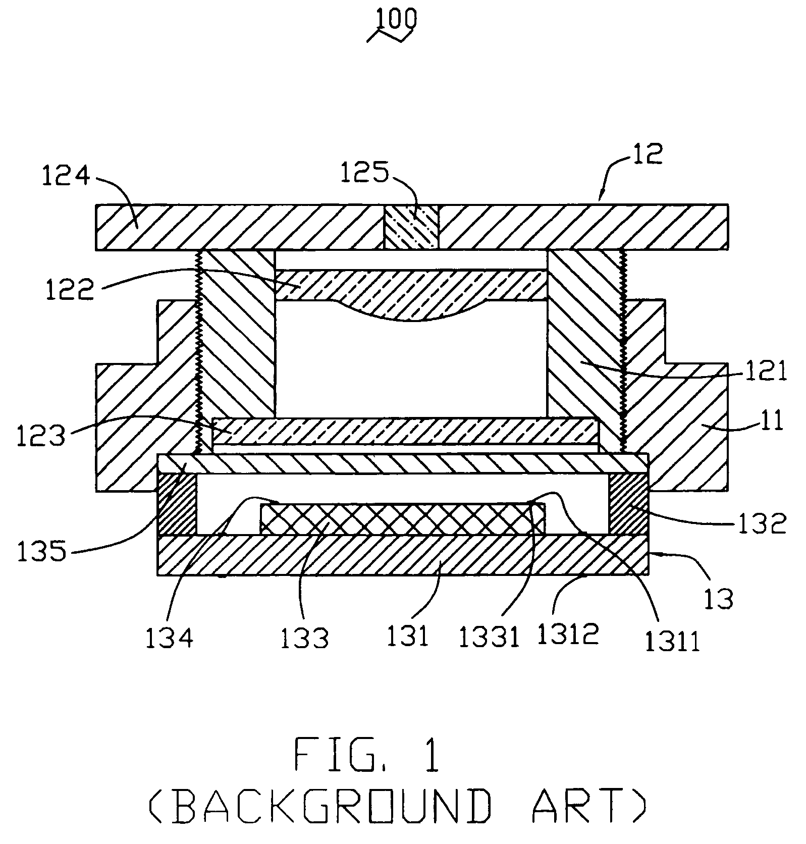
a technology of image sensor and camera module, which is applied in the field of digital camera modules, can solve the problems that the digital camera module b>100/b> is not suitable for slim, compact electronic products
- Summary
- Abstract
- Description
- Claims
- Application Information
AI Technical Summary
Benefits of technology
Problems solved by technology
Method used
Image
Examples
first embodiment
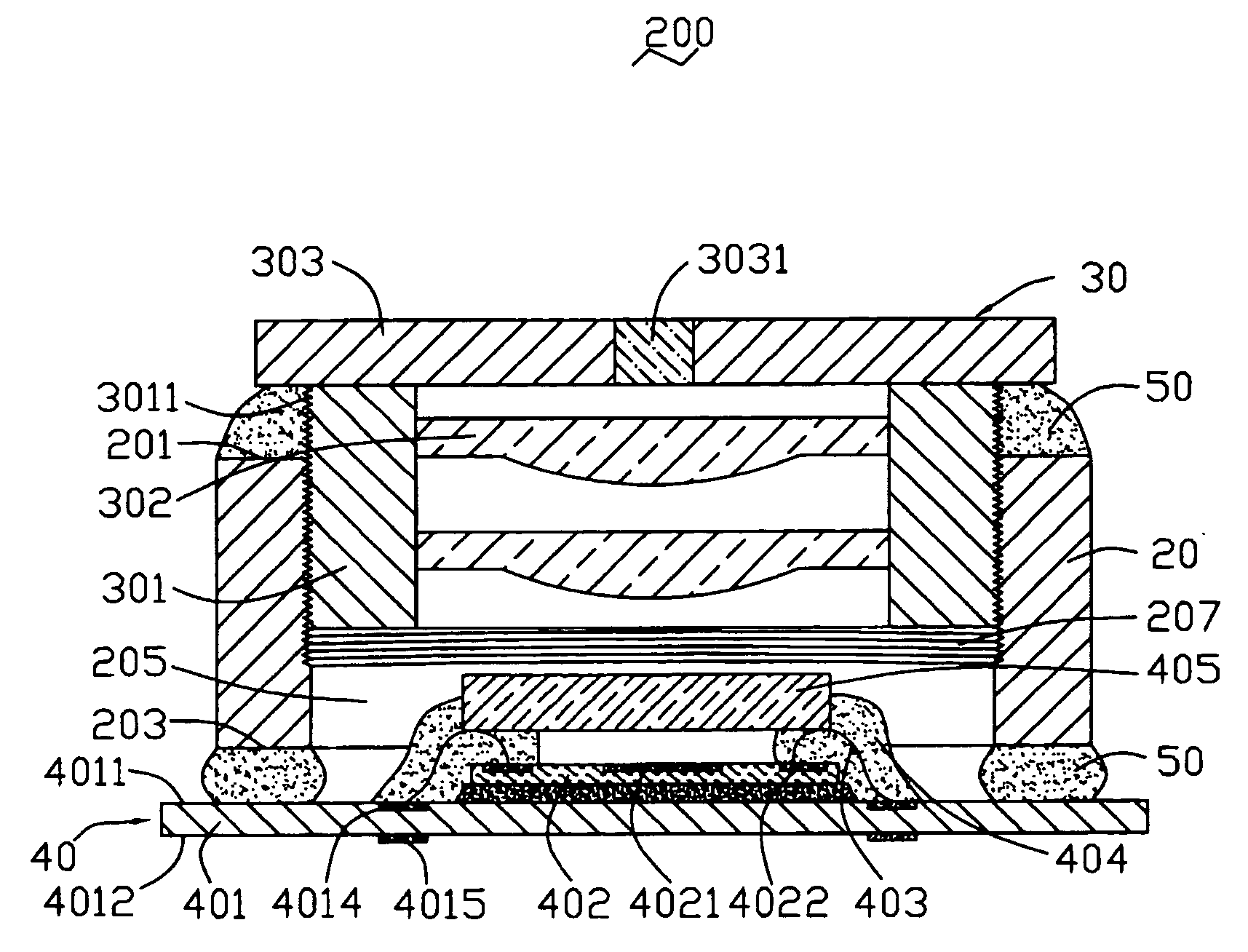
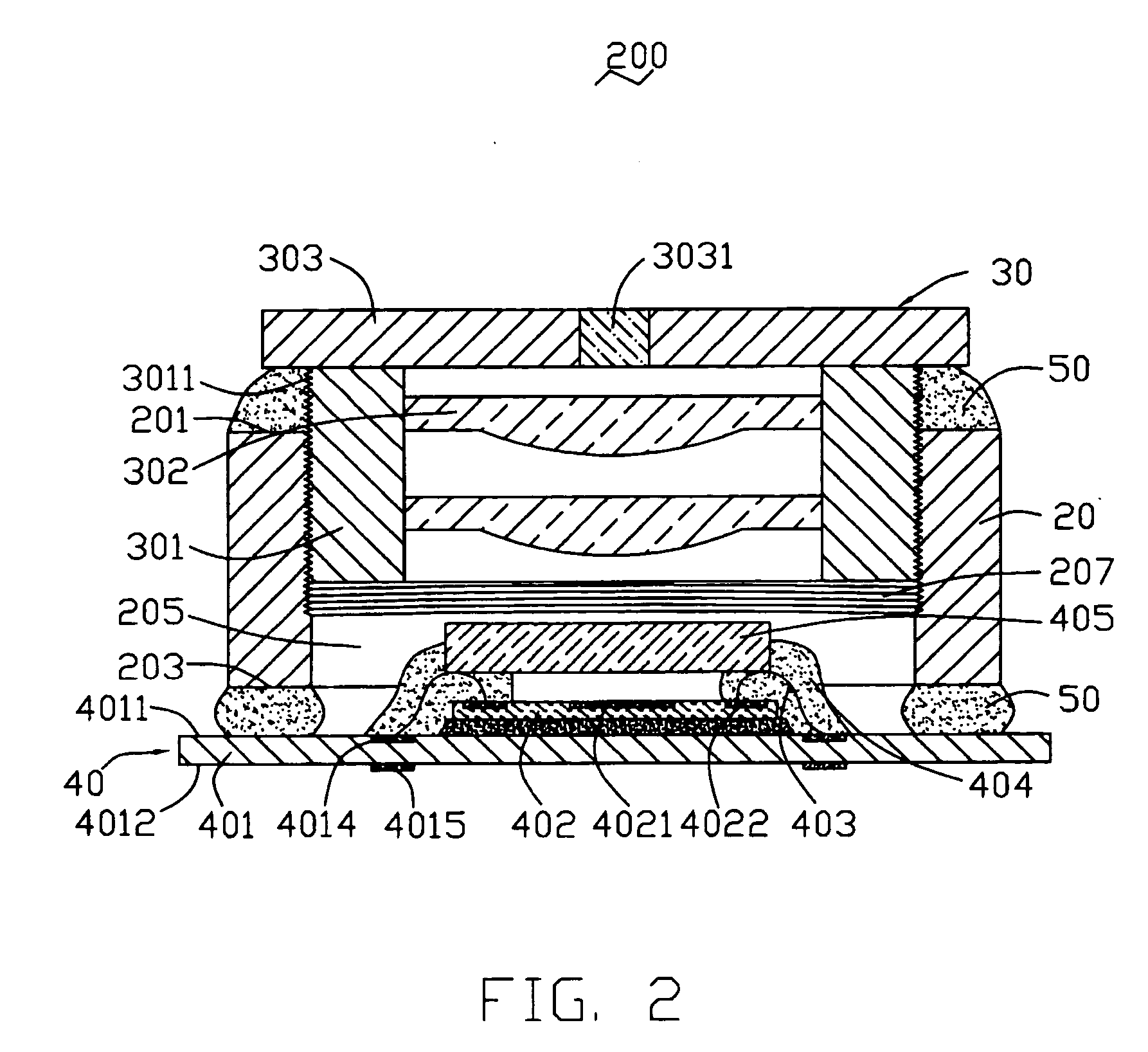
[0014] Referring to FIG. 2, a digital camera module 200 in accordance with the present invention is shown. The digital camera module 200 includes a lens holder 20, a lens module 30 and an image sensor chip package 40 both mounted on the lens holder 20.
[0015] The lens holder 20 has a front end 201, a rear end 203 opposite to the front end 201, and a receiving cavity 205 penetrating through the lens holder 20 from the front end 201 to the rear end 203. An internal thread 207 is formed on an inner periphery surface the lens holder 20.
[0016] The lens module 30 includes a barrel 301 and at least one lens 302. The barrel 301 is a hollow cylinder for receiving the at least one lens 302 therein, and has an external thread 3011 formed on an external surface thereof. One end of the barrel 301 is covered by a plate 303 which has a transparent region 3031 formed in a central portion thereof. The transparent region 3031 aligns with an optical axis of the lens 302 allowing light to be transmitte...
second embodiment
[0025] In the present invention as shown in FIG. 3, a digital camera module 300 has a similar structure to the digital camera module 200. The digital camera module 300 includes a lens holder 22, a lens module 32 and an image sensor chip package 42. The lens holder 22 includes a front end 221, a rear end 223, a hole 225 and an internal thread 227. The lens module 32 is configured to have a lens barrel 321 having an external thread 3211, at least one lens 322 and a plate 323 having a transparent region 3231 formed at a central portion of the plate 323. The image sensor chip package 42 includes a base 421 having a top surface 4211, a bottom surface 4212, a plurality of top pads 4214 and a plurality of bottom pads 4215, an image sensor chip 422 including a photosensitive area 4221 and a plurality of chip pads 4222, a plurality of wires 423, an adhesive means 424 and a transparent board 425.
[0026] The difference between the image sensor chip package 300 and the image sensor chip package ...
PUM
 Abstract
Description
Claims
Application Information
 - R&D
- Intellectual Property
- Life Sciences
- Materials
- Tech Scout
- Unparalleled Data Quality
- Higher Quality Content
- 60% Fewer Hallucinations
Browse by: Latest US Patents, China's latest patents, Technical Efficacy Thesaurus, Application Domain, Technology Topic, Popular Technical Reports.
© 2025 PatSnap. All rights reserved.Legal|Privacy policy|Modern Slavery Act Transparency Statement|Sitemap|About US| Contact US: help@patsnap.com


