Processor circuit and method of allocating a logic chip to a memory chip

a logic chip and logic circuit technology, applied in the field of processing circuits, can solve the problems of inability to remove the non-volatile memory from the integrated circuit, which includes both the non-volatile memory and the logic circuit, and cannot be 100 percent compatible with the production process of memories, and logic circuits cannot be generated at maximum speed

Inactive Publication Date: 2006-12-28
INFINEON TECH AG
View PDF16 Cites 13 Cited by
  • Summary
  • Abstract
  • Description
  • Claims
  • Application Information

AI Technical Summary

Problems solved by technology

Particularly for security-relevant applications, but also when other access limitations of any type exist, wherein these access limitations are stored, for example, in the non-volatile memory, which means when generally the access to the CPU or logic circuit, respectively, is regulated by data stored in the NVM, an attack to this access regulation would be, for example, to remove or delete non-volatile memory or to write other data on the same.
Removing the non-volatile memory from the integrated circuit, which includes both the non-volatile memory and the logic circuit, however, is not possible.
On the other hand, it is known that the production processes for logic circuits are not a hundred percent compatible with the production processes for memories.
This means that certain production steps are required for memory production, which again results in the fact that logic circuits cannot be generated with maximum speed.
On the other hand, when logic circuits are to be produced with maximum speed, production steps can be required which again cause the generated memory to have a lower quality or to be slower or less densely packed.
Thus, it has been found out that it is generally more expensive to integrate both logic elements and memory elements on a chip, as in the case of chip cards.
On the other hand, in such a case, an attacker could also be able to run his own code on the chip by deleting the original memory chip, which again could have the effect that he can illegally use access-limited functions of the chip and possibly spy them out.

Method used


Image

  • Processor circuit and method of allocating a logic chip to a memory chip
  • Processor circuit and method of allocating a logic chip to a memory chip
  • Processor circuit and method of allocating a logic chip to a memory chip

Examples


Embodiment Construction

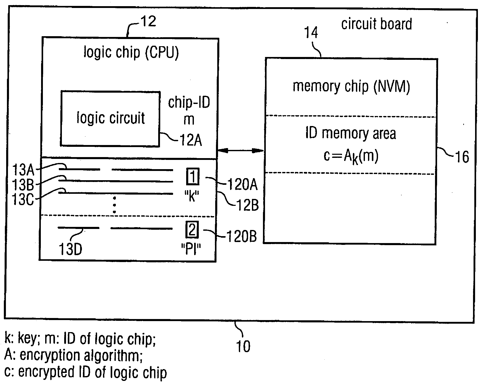
[0022]FIG. 1 shows an overview representation of a processor circuit according to the present invention. The processor circuit includes a carrier 10 which is a circuit board, particularly a printed circuit board in the preferred embodiment. A logic chip 12 on the one hand, and a memory chip 14 on the other hand are disposed on the circuit board. It should be noted that of course several logic chips or several memory chips, respectively, can be disposed. Logic chip 12, which can, for example, be a CPU, includes, on the one hand, a logic circuit 12a as well as a non-volatile memory 12b. The non-volatile memory 12b is divided into a first part 120a and into a second part 120b. In the first part 120a, a key k can be stored, while personalization information PI can be stored in the second part 120b. Preferably, the non-volatile memory 12b of the logic chip is designed as a fusing block, which means an array of individual fuses 13a, 13b, 13c, 13d. In the example shown in FIG. 1, the fuses...


PUM


Abstract

A processor circuit includes a logic chip with a logic circuit and a non-volatile memory as well as a memory chip with a non-volatile memory. A key is stored in the non-volatile memory of the logic chip by using electronic fuses. Further, personalization information is stored, which signalizes that the logic chip is allocated to a memory chip. A chip identification encrypted with the key is stored in the memory chip at an ID memory area. During starting up the processor, it is first verified whether the encrypted logic chip identification stored in the memory chip is authentic or not. Thereby, a simple and inexpensive personalization of a memory chip to a logic chip can be obtain in order to ward off attacks with regard to the removal or manipulation, respectively, of the memory chip.

Description

CROSS-REFERENCE TO RELATED APPLICATION [0001] This application is a continuation of copending International Application No. PCT / EP2004 / 008355, filed Jul. 26, 2004, which designated the United States and was not published in English.BACKGROUND OF THE INVENTION [0002] 1. Field of the Invention [0003] The present invention relates to processor circuits and particularly to a processor circuit with a logic chip and a memory chip. [0004] 2. Description of the Related Art [0005] Particularly in chip cards, normally, a non-volatile memory (NVM) is integrated on a chip with a CPU circuit. This means that the integrated circuit has both a memory area with memory transistors and a logic region with logic circuits forming the CPU. At the core, typical CPUs consist of logic circuits which are configured such that they can, on the one hand, perform the logic basic functions and, on the other hand, perform higher functions, such as adding, etc. Depending on the application, the logic circuits are ...

Claims


Application Information

Patent Timeline
Patent Type & Authority Applications(United States)
IPC IPC(8): G06K19/06G06F21/73G06F21/79G07F7/10
CPCG06F21/73G06F21/79G07F7/1008G06Q20/3576G06Q20/40975G06Q20/341
Inventor FISCHER, WIELANDSEIFERT, JEAN-PIERRE
Owner INFINEON TECH AG
Why Eureka
Try Eureka